

Prof. Hong Tang has devised a process of nanofabrication to create a silicon chip that contains all the components needed for a quantum information processor
“We can make a lot of these nanodevices easily by copying our design hundreds or thousands of times, without much additional effort or cost,” said Carsten Schuck, post-doctoral researcher and lead author of the paper. “It’s similar to what people in the semiconductor industry do, who developed the technology to make billions of transistors.”
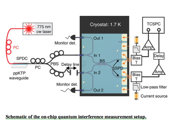
The two essential requirements for a scalable quantum information processor are quantum interference (in which a photon – able to be in more than one place at a time – crosses its own path) and single-photon detectors. The chip that the researchers designed contains a nanophotonic waveguide, which can guide light into small spaces and to wherever is needed on the chip. It also has a directional coupler that can split a light beam into two identical beams, or conversely, combine two beams into one output. Schuck compares his system to state-of-the-art experimental setups consisting of hundreds of bulky optical components to control a quantum system.
“Where we use a tiny silicon chip you used to need a whole room full of equipment to control a quantum system,” he said. “If you wanted to manipulate another quantum system, you needed another room and the money to buy all the equipment again. But if I want to manipulate another photon, I put an additional circuit on the same square-centimeter silicon chip, which takes a couple extra seconds during nanofabrication.”
With this research, Schuck said the research team should eventually realize a programmable optical quantum processor that can run a quantum algorithm. The scalability of the nanofabrication routines for silicon chips will then allow them to solve problems difficult for classical computers. He added that the same technology could also be useful for other applications, such as building extremely sensitive sensors or secure communication devices.
SOURCES -Yale, Nature Communications

Brian Wang is a Futurist Thought Leader and a popular Science blogger with 1 million readers per month. His blog Nextbigfuture.com is ranked #1 Science News Blog. It covers many disruptive technology and trends including Space, Robotics, Artificial Intelligence, Medicine, Anti-aging Biotechnology, and Nanotechnology.
Known for identifying cutting edge technologies, he is currently a Co-Founder of a startup and fundraiser for high potential early-stage companies. He is the Head of Research for Allocations for deep technology investments and an Angel Investor at Space Angels.
A frequent speaker at corporations, he has been a TEDx speaker, a Singularity University speaker and guest at numerous interviews for radio and podcasts. He is open to public speaking and advising engagements.