

In contrast to using advanced nanofabrication facilities based on chemical processing of materials, this flexible technique allows for rewritable “optical fabrication” of devices. This finding is likely to spawn new developments in emerging technologies such as low-power electronics based on the spin of electrons or ultrafast quantum computers.
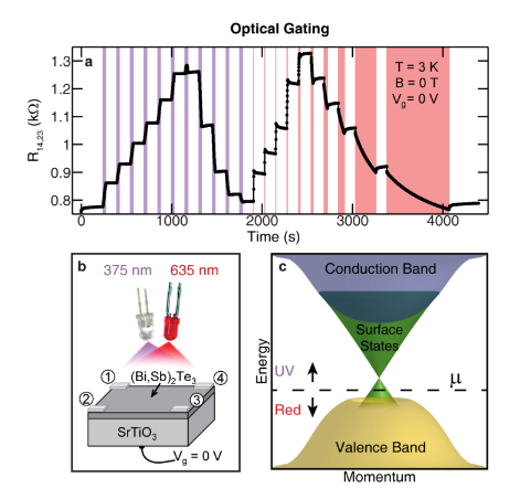
Topological insulators (TIs) have attracted much attention due to their spin-polarized surface and edge states, whose origin in symmetry gives them intriguing quantum-mechanical properties. Robust control over the chemical potential of TI materials is important if these states are to become useful in new technologies, or as a venue for exotic physics. Unfortunately, chemical potential tuning is challenging in TIs in part because the fabrication of electrostatic top-gates tends to degrade material properties and the addition of chemical dopants or adsorbates can cause unwanted disorder. Here, we present an all-optical technique which allows persistent, bidirectional gating of a (Bi,Sb)2Te3 channel by optically manipulating the distribution of electric charge below its interface with an insulating SrTiO3 substrate. In this fashion we optically pattern p-n junctions in a TI material, which we subsequently image using scanning photocurrent microscopy. The ability to dynamically write and re-write mesoscopic electronic structures in a TI may aid in the investigation of the unique properties of the topological insulating phase. The optical gating effect may be adaptable to other material systems, providing a more general mechanism for reconfigurable electronics.
Persistent optical gating of a TI channel
Arxiv – Persistent Optical Gating of a Topological Insulator
The electrons in topological insulators have unique quantum properties that many scientists believe will be useful for developing spin-based electronics and quantum computers. However, making even the simplest experimental circuits with these materials has proved difficult because traditional semiconductor engineering techniques tend to destroy their fragile quantum properties. Even a brief exposure to air can reduce their quality.
In Science Advances, the researchers report the discovery of an optical effect that allows them to “tune” the energy of electrons in these materials using light, and without ever having to touch the material itself. They have used it to draw and erase p-n junctions—one of the central components of a transistor—in a topological insulator for the first time.
Like many advances in science, the path to this discovery had an unexpected twist.
“To be honest, we were trying to study something completely different,” said Andrew Yeats, a graduate student in Awschalom’s laboratory and the paper’s lead author. “There was a slow drift in our measurements that we traced to a particular type of fluorescent lights in our lab. At first we were glad to be rid of it, and then it struck us—our room lights were doing something that people work very hard to do in these materials.”
The researchers went back to Bulley & Andrews Construction, the contractor that renovated the lab space, for more information about the lights. “I’ve never had a client so obsessed with the overhead lighting,” said Frank Floss, superintendent for Bulley & Andrews. “I could have never imagined how important it would turn out to be.”
The researchers found that the surface of strontium titanate, the substrate material on which they had grown their samples, becomes electrically polarized when exposed to ultraviolet light, and their room lights happened to emit at just the right wavelength. The electric field from the polarized strontium titanate was leaking into the topological insulator layer, changing its electronic properties.
Awschalom and his colleagues found that by intentionally focusing beams of light on their samples, they could draw electronic structures that persisted long after the light was removed.
“It’s like having a sort of quantum Etch A Sketch in our lab,” he said. They also found that bright red light counteracted the effect of the ultraviolet light, allowing them to both write and erase. “Instead of spending weeks in the cleanroom and potentially contaminating our materials,” said Awschalom, “now we can sketch and measure devices for our experiments in real time. When we’re done, we just erase it and make something else. We can do this in less than a second.”
To test whether the new technique might interfere with the unique properties of topological insulators, the team measured their samples in high magnetic fields. They found promising signatures of an effect called weak anti-localization, which arises from quantum interference between the different simultaneous paths that electrons can take through a material when they behave as waves.
“One exciting aspect of this work is that it’s noninvasive,” said Prof. Nitin Samarth, the George A. and Margaret M. Downsbrough Department Head of Physics at Penn State, and a lead researcher on the project. “Since the electrical polarization occurs in an adjacent material, and the effect persists in the dark, the topological insulator remains relatively undisturbed. With these fragile quantum materials, sometimes you have to use a light touch.”
To better understand the physics behind the effect, the researchers conducted a number of control measurements. They showed that the optical effect is not unique to topological insulators, but that it can act on other materials grown on strontium titanate as well.
“In a way, the most exciting aspect of this work is that it should be applicable to a wide range of nanoscale materials such as complex oxides, graphene and transition metal dichalcogenides,” said Awschalom. “It’s not just that it’s faster and easier. This effect could allow electrical tuning of materials in a wide range of optical, magnetic and spectroscopic experiments where electrical contacts are extremely difficult or simply impossible.”
SOURCES – University of Chicago, Arxiv, Scientific Advances

Brian Wang is a Futurist Thought Leader and a popular Science blogger with 1 million readers per month. His blog Nextbigfuture.com is ranked #1 Science News Blog. It covers many disruptive technology and trends including Space, Robotics, Artificial Intelligence, Medicine, Anti-aging Biotechnology, and Nanotechnology.
Known for identifying cutting edge technologies, he is currently a Co-Founder of a startup and fundraiser for high potential early-stage companies. He is the Head of Research for Allocations for deep technology investments and an Angel Investor at Space Angels.
A frequent speaker at corporations, he has been a TEDx speaker, a Singularity University speaker and guest at numerous interviews for radio and podcasts. He is open to public speaking and advising engagements.