
[EETimes] – Intel believes it can drive Moore’s Law down to 7 nanometers even without long-delayed advances in extreme ultraviolet lithography. It also gave its most detailed look to date at its foundry service for sharing its chipmaking prowess, including a description of a new low-cost alternative to 2.5D chip stacking it has in development.
Chipmakers generally don’t expect the much-delayed extreme ultraviolet (EUV) lithography in time for 10 nm chips, but many still hold out hopes it could be ready for a 7 nm generation.
Mark Bohr did not give any hints about how Intel will make 7 or even 10 nm chips without EUV. However he did note at 14 nm Intel is using triple patterning on one or more critical layers.
Although wafer costs rose at an accelerating rate for the last two nodes due to the need for more masks, Intel continues to pack more transistors in a given area of silicon. The density offsets wafer costs, leading to the cost-per-transistor decline, Bohr said in his talk on Intel’s 14 nm process.
Intel already announced it has started making in volume chips using a 14 nm process at a lower cost per transistor than its prior 22 nm generation. It also said it is in development of a 10 nm process that it believes will deliver lower cost per transistor.
In a separate talk, Intel said before the end of 2015 it could offer external foundry customers a chance to try out its emerging 10 nm process on shared wafers called shuttles.
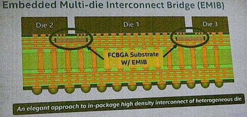
Most significantly, Intel is far along in testing a lower-cost alternative to 2.5D chip stacks it calls the Embedded Multi-Die Interconnect Bridge.

Unlike the 2.5D process, EMIB does not lay dies side-by-side on large silicon interposers, connecting them with through silicon vias (TSVs). Instead it uses a more conventional kind of flip chip process with metal bump interconnects inside a package.
EMIB employs back-end-of-line metallization and wafer thinning techniques used in a 2.5D stack. However by eliminating TSVs it significantly reduces costs, including costs of wasted die, Rikhi said. The process offers interconnects that are as dense and fast as TSVs, he added.

Intel has prototyped chips with “far north of five die” linked in an EMIB package. It expects to sample the technique to foundry customers in 2015.
If you liked this article, please give it a quick review on ycombinator or StumbleUpon. Thanks

Brian Wang is a Futurist Thought Leader and a popular Science blogger with 1 million readers per month. His blog Nextbigfuture.com is ranked #1 Science News Blog. It covers many disruptive technology and trends including Space, Robotics, Artificial Intelligence, Medicine, Anti-aging Biotechnology, and Nanotechnology.
Known for identifying cutting edge technologies, he is currently a Co-Founder of a startup and fundraiser for high potential early-stage companies. He is the Head of Research for Allocations for deep technology investments and an Angel Investor at Space Angels.
A frequent speaker at corporations, he has been a TEDx speaker, a Singularity University speaker and guest at numerous interviews for radio and podcasts. He is open to public speaking and advising engagements.


