

Normally, electrons travel through a material in a way that is similar to the motion of electromagnetic waves, including light; their behavior can be described by wave equations. That led the MIT researchers to the idea of harnessing the cloaking mechanisms developed to shield objects from view — but applying it to the movement of electrons, which is key to electronic and thermoelectric devices.
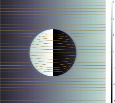
Diagram shows the ‘probability flux’ of electrons, a representation of the paths of electrons as they pass through an ‘invisible’ nanoparticle. While the paths are bent as they enter the particle, they are subsequently bent back so that they re-emerge from the other side on the same trajectory they started with — just as if the particle wasn’t there. Image courtesy Bolin Liao et al.
Physical Review Letters – Cloaking Core-Shell Nanoparticles from Conducting Electrons in Solids
Previous work on cloaking objects from view has relied on so-called metamaterials made of artificial materials with unusual properties. The composite structures used for cloaking cause light beams to bend around an object and then meet on the other side, resuming their original path — making the object appear invisible.
“We were inspired by this idea,” says Chen, the Carl Richard Soderberg Professor of Power Engineering at MIT, who decided to study how it might apply to electrons instead of light. But in the new electron-cloaking material developed by Chen and his colleagues, the process is slightly different.
The MIT researchers modeled nanoparticles with a core of one material and a shell of another. But in this case, rather than bending around the object, the electrons do actually pass through the particles: Their paths are bent first one way, then back again, so they return to the same trajectory they began with.
In computer simulations, the concept appears to work, Liao says. Now, the team will try to build actual devices to see whether they perform as expected. “This was a first step, a theoretical proposal,” Liao says. “We want to carry on further research on how to make some real devices out of this strategy.”
While the initial concept was developed using particles embedded in a normal semiconductor substrate, the MIT researchers would like to see if the results can be replicated with other materials, such as two-dimensional sheets of graphene, which might offer interesting additional properties.
The MIT researchers’ initial impetus was to optimize the materials used in thermoelectric devices, which produce an electrical current from a temperature gradient. Such devices require a combination of characteristics that are hard to obtain: high electrical conductivity (so the generated current can flow freely), but low thermal conductivity (to maintain a temperature gradient). But the two types of conductivity tend to coexist, so few materials offer these contradictory characteristics. The team’s simulations show this electron-cloaking material could meet these requirements unusually well.
The simulations used particles a few nanometers in size, matching the wavelength of flowing electrons and improving the flow of electrons at particular energy levels by orders of magnitude compared to traditional doping strategies. This might lead to more efficient filters or sensors, the researchers say. As the components on computer chips get smaller, Chen says, “we have to come up with strategies to control electron transport,” and this might be one useful approach.
The concept could also lead to a new kind of switches for electronic devices, Chen says. The switch could operate by toggling between transparent and opaque to electrons, thus turning a flow of them on and off. “We’re really just at the beginning,” he says. “We’re not sure how far this is going to go yet, but there is some potential” for significant applications.
Xiang Zhang, a professor of mechanical engineering at the University of California at Berkeley who was not involved in this research, says “this is very exciting work” that expands the concept of cloaking to the domain of electrons. The authors, he says, “uncovered a very interesting approach that may be very useful to thermoelectric applications.
ABSTRACT – In this Letter, we aim at making nanoparticles embedded in a host semiconductor with a size comparable to electronic wavelengths “invisible” to the electron transport. Inspired by the recent progress made in optics and working within the framework of the expansion of partial waves, we demonstrate that the opposite effects imposed by potential barriers and wells of a core-shell nanoparticle on the phase shifts associated with the scattered electron wave could make the scattering cross section of the first two partial waves vanish simultaneously. We show that this is sufficient to cloak the nanoparticle from being detected by electrons with specific energy in the sense that a total scattering cross section smaller than 0.01% of the physical cross section can be obtained and a 4 orders of magnitude difference in the total scattering cross section can be presented within an energy range of only 40 meV, indicating possible applications of the “electron cloaks” as novel electronic switches and sensors, and in efficient energy harvesting and conversion technologies.
Physics Synopsis – The design of artificial metamaterials that allow “cloaking”—apparent invisibility to acoustic and electromagnetic waves—is more than a party trick. Many applications suggest themselves if one could create cloaking at useful frequencies or in technologically relevant systems. Writing in Physical Review Letters, Bolin Liao and colleagues at Massachusetts Institute of Technology, Cambridge, propose the use of cloaking in semiconductor devices to optimize electron mobility in nanostructured materials.
As semiconductor devices are miniaturized to smaller and smaller sizes, having proper control over electron scattering and transport becomes more and more significant. Could one create scattering centers in a semiconductor that are transparent at certain energies? The team presents a description of core-shell nanoparticles in a semiconductor matrix host where the nanoparticles are of a similar size to the electron wavelength. The nanoparticles would then be invisible to electrons, improving the electron mobility at these energies, with associated tunability.
As an analogy to the Mie theory for electromagnetic scattering problems, the partial-wave formalism expresses the total scattering cross section as a summation of contributions from “partial waves” with different angular momenta. To be practical, the nanoparticles would be of a similar size to the electron wavelength; thus higher order partial waves would inevitably contribute. Working under this framework, they adjust the electron wavelengths, the core-shell ratio, and the effective mass of the core and shell materials to achieve four orders of magnitude decrease in scattering within a narrow energy range. Liao et al. suggest an implementation that involves a gallium arsenide two-dimensional system, as well as a three-dimensional scheme involving thermoelectric materials. Possible applications of these “electron cloaks” include novel electronic switches and sensors, and efficient energy harvesting and conversion techniques.
If you liked this article, please give it a quick review on ycombinator or StumbleUpon. Thanks

Brian Wang is a Futurist Thought Leader and a popular Science blogger with 1 million readers per month. His blog Nextbigfuture.com is ranked #1 Science News Blog. It covers many disruptive technology and trends including Space, Robotics, Artificial Intelligence, Medicine, Anti-aging Biotechnology, and Nanotechnology.
Known for identifying cutting edge technologies, he is currently a Co-Founder of a startup and fundraiser for high potential early-stage companies. He is the Head of Research for Allocations for deep technology investments and an Angel Investor at Space Angels.
A frequent speaker at corporations, he has been a TEDx speaker, a Singularity University speaker and guest at numerous interviews for radio and podcasts. He is open to public speaking and advising engagements.