

The technique based on the switching properties of silicon oxide, a breakthrough discovery by Rice in 2008, was reported today in the online journal Nature Communications.
The Rice team led by chemist James Tour and physicist Douglas Natelson is making highly transparent, nonvolatile resistive memory devices based on the revelation that silicon oxide itself can be a switch. A voltage run across a thin sheet of silicon oxide strips oxygen atoms away from a channel 5 nanometers (billionths of a meter) wide, turning it into conductive metallic silicon. With lower voltages, the channel can then be broken and repaired repeatedly, over thousands of cycles.
That channel can be read as a “1″ or a “0,” which is a switch, the basic unit of computer memories. At 5 nm, it shows promise to extend Moore’s Law, which predicted computer circuitry will double in power every two years. Current state-of-the-art electronics are made with 22 nm circuits.

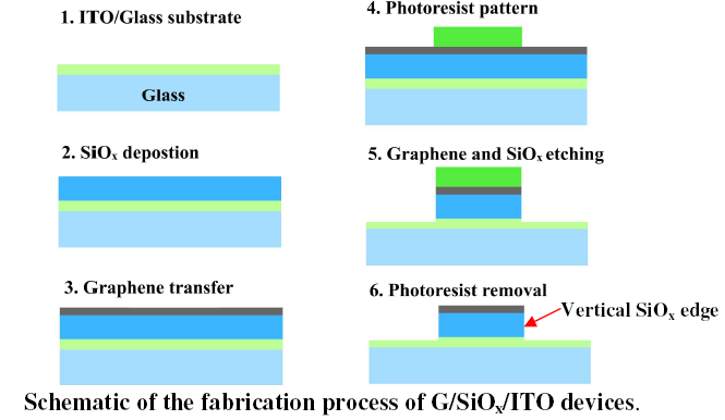
The research by Tour, Rice’s T.T. and W.F. Chao Chair in Chemistry as well as a professor of mechanical engineering and materials science and of computer science; lead author Jun Yao, a former graduate student at Rice and now a post-doctoral researcher at Harvard; Jian Lin, a Rice postdoctoral researcher, and their colleagues details memories that are 95 percent transparent, made of silicon oxide and crossbar graphene terminals on flexible plastic.
The Rice lab is making its devices with a working yield of about 80 percent, “which is pretty good for a non-industrial lab,” Tour said. “When you get these ideas into industries’ hands, they really sharpen it up from there.”
Manufacturers who have been able to fit millions of bits on small devices like flash memories now find themselves bumping against the physical limits of their current architectures, which require three terminals for each bit.
But the Rice unit, requiring only two terminals, makes it far less complicated. It means arrays of two-terminal memories can be stacked in three-dimensional configurations, vastly increasing the amount of information a memory chip might hold. Tour said his lab has also seen promise for making multi-state memories that would further increase their capacity.
Yao’s discovery followed work at Rice on graphitic-based memories in which researchers saw strips of graphite on a silicon oxide substrate break and heal when voltage was applied. Yao suspected the underlying silicon oxide was actually responsible, and he struggled to convince his lab colleagues. “Jun quietly continued his work and stacked up evidence, eventually building a working device with no graphite,” Tour said. “And still, others said, ‘Oh, it was exogenous carbon in the system that did it!’ Then he built it with no exposure to carbon on the chip.”
Yao’s paper detailing the silicon oxide mechanism appeared in Nature’s Scientific Reports in January.
His revelation became the basis for the next-generation memories being designed in Tour’s lab, where the team is building memories out of silicon oxides sandwiched between graphene – one-atom-thick ribbons of carbon – and attached to plastic sheets. There’s not a speck of metal in the entire unit (with the exception of leads attached to the graphene electrodes).
The marriage of silicon and graphene would extend the long-recognized utility of the first and prove once and for all the value of the second, long touted as a wonder material looking for a reason to be, Tour said. He noted the devices not only show potential for radiation-hardened devices – several built at Rice are now being evaluated at the International Space Station – but also withstand heat up to about 700 degrees Celsius. That means they can be mounted directly atop integrated processors with no ill effects.
The lab is also building crossbar memories with embedded diodes to better manipulate control voltages, Tour said. “We’ve been developing this slowly to understand the fundamental switching mechanisms,” he said. “Industries have flown in and looked at it, but we’re doing basic science here; we don’t package things nice and pretty, so what they see looks rudimentary.
“But this is now transitioning into an applied system that could well be taken up as a future memory system,” he said.
ABSTRACT – Transparent electronic memory would be useful in integrated transparent electronics. However, achieving such transparency produces limits in material composition, and hence, hinders processing and device performance. Here we present a route to fabricate highly transparent memory using SiOx as the active material and indium tin oxide or graphene as the electrodes. The two-terminal, nonvolatile resistive memory can also be configured in crossbar arrays on glass or flexible transparent platforms. The filamentary conduction in silicon channels generated in situ in the SiOx maintains the current level as the device size decreases, underscoring their potential for high-density memory applications, and as they are two-terminal based, transitions to three-dimensional memory packages are conceivable. As glass is becoming one of the mainstays of building construction materials, and conductive displays are essential in modern handheld devices, to have increased functionality in form-fitting packages is advantageous.
9 pages of supplemental information
If you liked this article, please give it a quick review on ycombinator or StumbleUpon. Thanks

Brian Wang is a Futurist Thought Leader and a popular Science blogger with 1 million readers per month. His blog Nextbigfuture.com is ranked #1 Science News Blog. It covers many disruptive technology and trends including Space, Robotics, Artificial Intelligence, Medicine, Anti-aging Biotechnology, and Nanotechnology.
Known for identifying cutting edge technologies, he is currently a Co-Founder of a startup and fundraiser for high potential early-stage companies. He is the Head of Research for Allocations for deep technology investments and an Angel Investor at Space Angels.
A frequent speaker at corporations, he has been a TEDx speaker, a Singularity University speaker and guest at numerous interviews for radio and podcasts. He is open to public speaking and advising engagements.