
Scientists at the Naval Research Laboratory have demonstrated, for the first time, the use of graphene as a tunnel barrier — an electrically insulating barrier between two conducting materials through which electrons tunnel quantum mechanically. They report fabrication of magnetic tunnel junctions using graphene, a single atom thick sheet of carbon atoms arranged in a honeycomb lattice, between two ferromagnetic metal layers in a fully scalable photolithographic process. Their results demonstrate that single-layer graphene can function as an effective tunnel barrier for both charge and spin-based devices, and enable realization of more complex graphene-based devices for highly functional nanoscale circuits, such as tunnel transistors, non-volatile magnetic memory and reprogrammable spin logic.

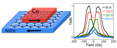
Diagram (left) of the graphene-based magnetic tunnel junction, where a single atom thick layer of carbon atoms in a honeycomb lattice separates two magnetic metal films (cobalt and permalloy). The magnetizations of the films can be aligned parallel or antiparallel, resulting in a change in resistance for current flowing through the structure, called the tunnel magnetoresistance (TMR). The plot (right) shows the TMR as an applied magnetic field changes the relative orientation of the magnetizations — the TMR persists well above room temperature.
(U.S. Naval Research Laboratory)
Nanoletters – Graphene As a Tunnel Barrier: Graphene-Based Magnetic Tunnel Junctions
The research initiates a “paradigm shift in tunnel barrier technology for magnetic tunnel junctions (MTJs) used for advanced sensors, memory and logic,” explains NRL’s Dr. Berend Jonker. Graphene has been the focus of intense research activity because of its remarkable electronic and mechanical properties. In the past, researchers focused on developing graphene as a conductor, or perhaps a semiconductor, where the current flows in-plane parallel to the carbon honeycomb sheet. In contrast, the NRL researchers show that graphene serves as an excellent tunnel barrier when current is directed perpendicular to the plane, and in fact, also preserves the spin polarization of the tunneling current.
Tunnel barriers are the basis for many electronic (charge-based) and spintronic (spin-based) device structures. Fabrication of ultra-thin and defect-free barriers is an ongoing challenge in materials science. Typical tunnel barriers are based on metal oxides (e.g. aluminum oxide or magnesium oxide), and issues such as non-uniform thicknesses, pinholes, defects and trapped charge compromise their performance and reliability. Such oxide tunnel barriers have several limitations which hinder future performance. For example, they have high resistance-area (RA) products which results in higher power consumption and local heating; they allow interdiffusion at the interfaces, which reduces their performance and can lead to catastrophic failure; and their thickness is generally non-uniform, resulting in “hot spots” in the current transport. In contrast, Dr. Jonker explains, the inherent material properties of graphene make it an ideal tunnel barrier. Graphene is chemically inert and impervious to diffusion even at high temperatures. The atomic thickness of graphene represents the ultimate in tunnel barrier scaling for the lowest possible RA product, lowest power consumption and fastest switching speed.
This discovery by NRL researchers is significant because MTJs are widely utilized as read heads in the hard disk drive found in every computer, and as memory elements in non-volatile magnetic random access memory (MRAM) which is rapidly emerging as a universal memory replacement for the many varieties of conventional semiconductor-based memory. They are also considered to be lead contenders as reprogrammable, non-volatile elements for a universal logic block.
Although there has been significant progress, the emerging generation of MTJ-based MRAM relies upon spin-transfer torque switching, and is severely limited by the unacceptably high current densities required to switch the logic state of the cell. The accompanying issues of power consumption and thermal dissipation prevent scaling to higher densities and operation at typical CMOS voltages. The 2011 International Technology Roadmap for Semiconductors (ITRS) states that “all of the existing forms of nonvolatile memory face limitations based on material properties. Success will hinge on finding and developing alternative materials and/or developing alternative emerging technologies … development of electrically accessible non-volatile memory with high speed and high density would initiate a revolution in computer architecture … and provide a significant increase in information throughput beyond the traditional benefits of scaling when fully realized for nanoscale CMOS devices” (ITRS 2011 Executive Summary, p28; and Emerging Research Devices, p. 4).
NRL researchers believe that the graphene-based magnetic tunnel junctions they have demonstrated will eclipse the performance and ease of fabrication of existing oxide technology. These graphene-based MTJs would be a breakthrough for nascent spin-based technologies like MRAM and spin logic, and enable the electrically accessible non-volatile memory required to initiate a revolution in computer architecture. These results also pave the way for utilization of other two-dimensional materials such as hexagonal boron nitride for similar applications.
ABSTRACT – Graphene has been widely studied for its high in-plane charge carrier mobility and long spin diffusion lengths. In contrast, the out-of-plane charge and spin transport behavior of this atomically thin material have not been well addressed. We show here that while graphene exhibits metallic conductivity in-plane, it serves effectively as an insulator for transport perpendicular to the plane. We report fabrication of tunnel junctions using single-layer graphene between two ferromagnetic metal layers in a fully scalable photolithographic process. The transport occurs by quantum tunneling perpendicular to the graphene plane and preserves a net spin polarization of the current from the contact so that the structures exhibit tunneling magnetoresistance to 425 K. These results demonstrate that graphene can function as an effective tunnel barrier for both charge and spin-based devices and enable realization of more complex graphene-based devices for highly functional nanoscale circuits, such as tunnel transistors, nonvolatile magnetic memory, and reprogrammable spin logic.
If you liked this article, please give it a quick review on ycombinator or StumbleUpon. Thanks

Brian Wang is a Futurist Thought Leader and a popular Science blogger with 1 million readers per month. His blog Nextbigfuture.com is ranked #1 Science News Blog. It covers many disruptive technology and trends including Space, Robotics, Artificial Intelligence, Medicine, Anti-aging Biotechnology, and Nanotechnology.
Known for identifying cutting edge technologies, he is currently a Co-Founder of a startup and fundraiser for high potential early-stage companies. He is the Head of Research for Allocations for deep technology investments and an Angel Investor at Space Angels.
A frequent speaker at corporations, he has been a TEDx speaker, a Singularity University speaker and guest at numerous interviews for radio and podcasts. He is open to public speaking and advising engagements.