
Working at a scale applicable to infrared light, the Harvard team has used extremely short and powerful laser pulses to create three-dimensional patterns of tiny silver dots within a material. Those suspended metal dots are essential for building futuristic devices like invisibility cloaks.
“If you want a bulk metamaterial for visible and infrared light, you need to embed particles of silver or gold inside a dielectric, and you need to do it in 3D, with high resolution,” says lead author Kevin Vora, a graduate student at the Harvard School of Engineering and Applied Sciences (SEAS).
“This work demonstrates that we can create silver dots that are disconnected in x, y, and z,” Vora says. “There’s no other technique that feasibly allows you to do that. Being able to make patterns of nanostructures in 3D is a very big step towards the goal of making bulk metamaterials.”

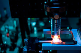
The experimental setup in Prof. Eric Mazur’s laser laboratory at Harvard. Using femtosecond lasers, Mazur and colleagues have developed a new nanofabrication process for use in creating metamaterials.
When a conventional laser shines on a transparent material, the light passes straight through, with slight refraction. The femtosecond laser is special because it emits a burst of photons as bright as the surface of the sun in a flash lasting only 50 quadrillionths (5 × 10^-14) of a second. Instead of shining through the material, that energy gets trapped within it, exciting the electrons within the material and achieving a phenomenon known as nonlinear absorption.
Inside the pocket where that energy is trapped, a chemical reaction can take place, permanently altering the internal structure of the material. The process has previously been exploited for 2D and simple 3D metal nanofabrication.
“Normally, when people use femtosecond lasers in fabrication, they’re creating a wood pile structure: something stacked on something else, being supported by something else,” explains Mazur.
“If you want to make an array of silver dots, however, they can’t float in space.”
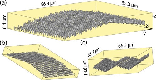
A new laser fabrication technique developed at Harvard allows for the creation of precisely arranged silver nanoparticles that are disconnected in 3D and supported by a polymer matrix. The new technique may prove critical in the development of metamaterials. Image courtesy of Kevin Vora.
In the new process, Vora, Mazur, and their colleagues combine silver nitrate, water, and a polymer called PVP into a solution, which they bake onto a glass slide. The solid polymer then contains ions of silver, which are photoreduced by the tightly focused laser pulses to form nanocrystals of silver metal, supported by the polymer matrix.
The need for this particular combination of chemicals, at the right concentrations, was not obvious in prior work. Researchers sometimes combine silver nitrate with water in order to create silver nanostructures, but that process provides no structural support for a 3D pattern. Another process combines silver nitrate, water, PVP, and ethanol, but the samples darken and degrade very quickly by producing silver crystals throughout the polymer.
With ethanol, the reaction happens too quickly and uncontrollably. Mazur’s team needed nanoscale crystals, precisely distributed and isolated in 3D.
“It was just a question of removing that reagent, and we got lucky,” Vora says. “What was most surprising about it was how simple it is. It was a matter of using less.”
We present a simple, one‐step technique for direct‐writing of a structured nanocomposite material with disconnected silver nanostructures in a polymer matrix. A nonlinear optical interaction between femtosecond laser pulses and a composite material creates silver structures that are embedded inside a polymer with submicrometer resolution (300 nm). We create complex patterns of silver nanostructures in three dimensions. The key to the process is the chemical composition of the sample that provides both a support matrix and controlled growth. The technique presented in this letter may offer a cost‐effective approach for the fabrication of bulk optical devices with engineered dispersion.
If you liked this article, please give it a quick review on ycombinator or StumbleUpon. Thanks

Brian Wang is a Futurist Thought Leader and a popular Science blogger with 1 million readers per month. His blog Nextbigfuture.com is ranked #1 Science News Blog. It covers many disruptive technology and trends including Space, Robotics, Artificial Intelligence, Medicine, Anti-aging Biotechnology, and Nanotechnology.
Known for identifying cutting edge technologies, he is currently a Co-Founder of a startup and fundraiser for high potential early-stage companies. He is the Head of Research for Allocations for deep technology investments and an Angel Investor at Space Angels.
A frequent speaker at corporations, he has been a TEDx speaker, a Singularity University speaker and guest at numerous interviews for radio and podcasts. He is open to public speaking and advising engagements.