
A University of Manchester team lead by Nobel laureates Professor Andre Geim and Professor Konstantin Novoselov has literally opened a third dimension in graphene research. Their research shows a transistor that may prove the missing link for graphene to become the next silicon.
Graphene – one atomic plane of carbon – is a remarkable material with endless unique properties, from electronic to chemical and from optical to mechanical.
One of many potential applications of graphene is its use as the basic material for computer chips instead of silicon. This potential has alerted the attention of major chip manufactures, including IBM, Samsung, Texas Instruments and Intel. Individual transistors with very high frequencies (up to 300 GHz) have already been demonstrated by several groups worldwide.
Unfortunately, those transistors cannot be packed densely in a computer chip because they leak too much current, even in the most insulating state of graphene. This electric current would cause chips to melt within a fraction of a second.
Tunnelling transistor based on vertical graphene heterostructures. Tunnelling current between two graphene layers can be controlled by gating
Science – Field-Effect Tunneling Transistor Based on Vertical Graphene Heterostructures
An obstacle to the use of graphene as an alternative to silicon electronics has been the absence of an energy gap between its conduction and valence bands, which makes it difficult to achieve low power dissipation in the OFF state. We report a bipolar field-effect transistor that exploits the low density of states in graphene and its one atomic layer thickness. Our prototype devices are graphene heterostructures with atomically thin boron nitride or molybdenum disulfide acting as a vertical transport barrier. They exhibit room temperature switching ratios of ≈50 and ≈10,000 respectively. Such devices have potential for high-frequency operation and large-scale integration.
The University of Manchester scientists now suggest using graphene not laterally (in plane) – as all the previous studies did – but in the vertical direction. They used graphene as an electrode from which electrons tunnelled through a dielectric into another metal. This is called a tunnelling diode.
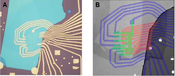
One of our hBN‐graphene‐hBN‐graphene‐hBN devices. (A) Optical image of the final device.
(B) Electron micrograph of the same device at the final design stage before evaporating Au leads. Two 10‐terminal Hall bars made from graphene are shown in green and orange. The spatial scale is given by the width of the Hall bar, which was 2 micron for this device. Fabrication required 4 dry transfers and alignments of the graphene and hBN crystals, 4 nonconsecutive rounds of electron‐beam lithography, 3 rounds of plasma etching and two separate metal depositionsThen they exploited a truly unique feature of graphene – that an external voltage can strongly change the energy of tunnelling electrons. As a result they got a new type of a device – vertical field-effect tunnelling transistor in which graphene is a critical ingredient.
Dr Leonid Ponomarenko, who spearheaded the experimental effort, said: “We have proved a conceptually new approach to graphene electronics. Our transistors already work pretty well. I believe they can be improved much further, scaled down to nanometre sizes and work at sub-THz frequencies.”
“It is a new vista for graphene research and chances for graphene-based electronics never looked better than they are now”, adds Professor Novoselov.
Graphene alone would not be enough to make the breakthrough. Fortunately, there are many other materials, which are only one atom or one molecule thick, and they were used for help.
The Manchester team made the transistors by combining graphene together with atomic planes of boron nitride and molybdenum disulfide. The transistors were assembled layer by layer in a desired sequence, like a layer cake but on an atomic scale.
Such layer-cake superstructures do not exist in nature. It is an entirely new concept introduced in the report by the Manchester researchers. The atomic-scale assembly offers many new degrees of functionality, without some of which the tunnelling transistor would be impossible.
“The demonstrated transistor is important but the concept of atomic layer assembly is probably even more important,” explains Professor Geim.
Professor Novoselov added: “Tunnelling transistor is just one example of the inexhaustible collection of layered structures and novel devices which can now be created by such assembly.
“It really offers endless opportunities both for fundamental physics and for applications. Other possible examples include light emission diodes, photovoltaic devices, and so on.”
11 pages of supplemental material
If you liked this article, please give it a quick review on ycombinator or StumbleUpon. Thanks

Brian Wang is a Futurist Thought Leader and a popular Science blogger with 1 million readers per month. His blog Nextbigfuture.com is ranked #1 Science News Blog. It covers many disruptive technology and trends including Space, Robotics, Artificial Intelligence, Medicine, Anti-aging Biotechnology, and Nanotechnology.
Known for identifying cutting edge technologies, he is currently a Co-Founder of a startup and fundraiser for high potential early-stage companies. He is the Head of Research for Allocations for deep technology investments and an Angel Investor at Space Angels.
A frequent speaker at corporations, he has been a TEDx speaker, a Singularity University speaker and guest at numerous interviews for radio and podcasts. He is open to public speaking and advising engagements.