

A team of scientists, led by Guillaume Gervais from McGill’s Physics Department and Mike Lilly from Sandia National Laboratories, has engineered one of the world’s smallest electronic circuits. It is formed by two wires separated by only about 150 atoms or 15 nanometers (nm). This discovery, published in the journal Nature Nanotechnology, could have a significant effect on the speed and power of the ever smaller integrated circuits of the future in everything from smartphones to desktop computers, televisions and GPS systems.
This is the first time that anyone has studied how the wires in an electronic circuit interact with one another when packed so tightly together. Surprisingly, the authors found that the effect of one wire on the other can be either positive or negative. This means that a current in one wire can produce a current in the other one that is either in the same or the opposite direction. This discovery, based on the principles of quantum physics, suggests a need to revise our understanding of how even the simplest electronic circuits behave at the nanoscale
In addition to the effect on the speed and efficiency of future electronic circuits, this discovery could also help to solve one of the major challenges facing future computer design. This is managing the ever-increasing amount of heat produced by integrated circuits. Well-known theorist Markus Büttiker speculates that it may be possible to harness the energy lost as heat in one wire by using other wires nearby. Moreover, Buttiker believes that these findings will have an impact on the future of both fundamental and applied research in nanoelectronics.

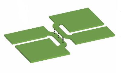
Schematics of the fabrication process of the vertically coupled quantum circuits.
Electron interactions in and between wires become increasingly complex and important as circuits are scaled to nanometre sizes, or use reduced-dimensional conductors such as carbon nanotubes, nanowires and gated high-mobility two-dimensional electron systems. This is because the screening of the long-range Coulomb potential of individual carriers is weakened in these systems, which can lead to phenomena such as Coulomb drag, where a current in one wire induces a voltage in a second wire through Coulomb interactions alone. Previous experiments have demonstrated Coulomb electron drag in wires separated by a soft electrostatic barrier of width more than 80 nm, which was interpreted as resulting entirely from momentum transfer. Here, we measure both positive and negative drag between adjacent vertical quantum wires that are separated by ~15 nm and have independent contacts, which allows their electron densities to be tuned independently. We map out the drag signal versus the number of electron sub-bands occupied in each wire, and interpret the results both in terms of momentum-transfer and charge-fluctuation induced transport models. For wires of significantly different sub-band occupancies, the positive drag effect can be as large as 25%.
Voltage increases up to 25% observed in closely packed nanowires at Sandia Labs
Unexpected voltage increases of up to 25 percent in two barely separated nanowires have been observed at Sandia National Laboratories.
Designers of next-generation devices using nanowires to deliver electric currents — including telephones, handheld computers, batteries and certain solar arrays — may need to make allowances for such surprise boosts.
“People have been working on nanowires for 20 years,” says Sandia lead researcher Mike Lilly. “At first, you study such wires individually or all together, but eventually you want a systematic way of studying the integration of nanowires into nanocircuitry. That’s what’s happening now. It’s important to know how nanowires interact with each other rather than with regular wires.”
Though the gallium-arsenide nanowire structures used by Lilly’s team are fragile, nanowires in general have very practical characteristics — they may crack less than their bigger cousins, they’re cheaper to produce and they offer better electronic control.
For years, the best available test method required researchers to put a charged piece of material called a gate between two nanowires on a single shelf. The gate, flooded with electrons, acted as a barrier: It maintained the integrity, in effect, of the wires on either side of it by repelling any electrons attempting to escape across it. But the smallest wire separation allowed by the gate was 80 nanometers. Nanowires in future devices will be packed together much more closely, so a much smaller gap was necessary for testing.
The current test design has the brilliance of simplicity. What Lilly and co-workers at McGill University in Montreal envisioned was to put the nanowires one above the other, rather than side by side, by separating them with a few atomic layers of extremely pure, home-grown crystal. This allowed them to test nanowires separated vertically by only 15 nanometers — about the distance next-generation devices are expected to require. And because each wire sits on its own independent platform, each can be independently fed and controlled by electrical inputs varied by the researchers.
While applications for technical devices interest Lilly, it’s the characteristics of nanowires as a problem in one-dimensional (1-D) basic science that fascinates him.
A 1-D wire is not your common, thick-waisted, 3-D household wire, which allows current to move horizontally, vertically, and forward; nor is it your smaller, flattened micron-sized 2-D wires in typical electronic devices that allow electrons to move forward and across but not up and down. In 1-D wires, the electrons can only move in one direction: forward, like prisoners coming to lunch, one behind the other.
“In the long run, our test device will allow us to probe how 1-D conductors are different from 2-D and 3-D conductors,” Lilly said. “They are expected to be very different, but there are relatively few experimental techniques that have been used to study the 1-D ground state.”
One reason for the difference is the Coulomb force, responsible for what is termed the Coulomb “drag” effect, regardless of whether the force hastens or retards currents. Operating between wires, the force is inversely proportional to the square of the distance; that is, in ordinary microelectronics, the force is practically unnoticeable, but at nanodistances, the force is large enough that electrons in one wire can “feel” the individual electrons moving in another placed nearby.
If you liked this article, please give it a quick review on ycombinator or StumbleUpon. Thanks

Brian Wang is a Futurist Thought Leader and a popular Science blogger with 1 million readers per month. His blog Nextbigfuture.com is ranked #1 Science News Blog. It covers many disruptive technology and trends including Space, Robotics, Artificial Intelligence, Medicine, Anti-aging Biotechnology, and Nanotechnology.
Known for identifying cutting edge technologies, he is currently a Co-Founder of a startup and fundraiser for high potential early-stage companies. He is the Head of Research for Allocations for deep technology investments and an Angel Investor at Space Angels.
A frequent speaker at corporations, he has been a TEDx speaker, a Singularity University speaker and guest at numerous interviews for radio and podcasts. He is open to public speaking and advising engagements.