Nanoletters – Over the past 30 years electronic applications have been dominated by complementary metal oxide semiconductor (CMOS) devices. These combine p- and n-type field effect transistors (FETs) to reduce static power consumption. However, CMOS transistors are limited to static electrical functions, i.e., electrical characteristics that cannot be changed. Here we present the concept and a demonstrator of a universal transistor that can be reversely configured as p-FET or n-FET simply by the application of an electric signal. This concept is enabled by employing an axial nanowire heterostructure (metal/intrinsic-silicon/metal) with independent gating of the Schottky junctions. In contrast to conventional FETs, charge carrier polarity and concentration are determined by selective and sensitive control of charge carrier injections at each Schottky junction, explicitly avoiding the use of dopants as shown by measurements and calculations. Besides the additional functionality, the fabricated nanoscale devices exhibit enhanced electrical characteristics, e.g., record on/off ratio of up to 1 × 10^9 for Schottky transistors. This novel nanotransistor technology makes way for a simple and compact hardware platform that can be flexibly reconfigured during operation to perform different logic computations yielding unprecedented circuit design flexibility.
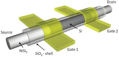
The reconfigurable transistor’s core consists of a nanowire structure embedded in a silicon dioxide shell. Electrons or holes flow from the source at one end of the nanowire through two gates to the drain at the other end of the nanowire. One gate is used to program the p- or n-polarity, whereas the other gate tunes the conductance through the nanowire. Image credit: ©Namlab gGmbH
Fabrication
In order to fabricate these devices, undoped silicon nanowires with <112> orientations were grown with an catalyst using the VLS method as described in Ref. 4. After etching the Au catalyst, the nanowires were dispersed in VLSI grade isopropanol by ultrasonic agitation and deposited on a 200 nm thick SiO2 layer residing on a p-Si substrate. Thermal oxidation at 875 °C took place to provide a surrounding SiO2 gate dielectric of approximately 10 nm thickness followed by forming gas anneal at 500 °C to passivate interface traps. The Ni reservoirs and source / drain connectors were patterned by electron-beam lithography. Thereby, the SiO2 nanowire shell was etched locally prior to Ni deposition. Upon annealing at 500 °C Ni diffuses axially into the nanowire within the SiO2 shell and transforms into metallic and single-crystalline NiSi2 as described in Ref. 5. Despite the presence of the oxide shell, the silicide intrudes axially into the nanowire. As a result, NiSi2 / intrinsic-Si / NiSi2 nanowire axial heterostructures surrounded by a SiO2 shell are formed. The location of the Schottky junctions is measured by scanning electron microscopy (SEM). Subsequently, individual metal top gate electrodes are patterned overlapping the Schottky junctions.
3 pages of supplemental information
If you liked this article, please give it a quick review on ycombinator or StumbleUpon. Thanks

Brian Wang is a Futurist Thought Leader and a popular Science blogger with 1 million readers per month. His blog Nextbigfuture.com is ranked #1 Science News Blog. It covers many disruptive technology and trends including Space, Robotics, Artificial Intelligence, Medicine, Anti-aging Biotechnology, and Nanotechnology.
Known for identifying cutting edge technologies, he is currently a Co-Founder of a startup and fundraiser for high potential early-stage companies. He is the Head of Research for Allocations for deep technology investments and an Angel Investor at Space Angels.
A frequent speaker at corporations, he has been a TEDx speaker, a Singularity University speaker and guest at numerous interviews for radio and podcasts. He is open to public speaking and advising engagements.


