
A research group at the NIMS International Center for Materials Nanoarchitectonics (MANA) proved that the electrical resistance of a metal single atomic layer on a silicon surface becomes zero by superconductivity. The work was done at 2.8K.
Focusing on an indium single atomic layer arranged with a special structure on a silicon surface, the team led by Dr. Uchihashi observed for the first time in the world that the electrical resistance of this substance become zero, and the substance displays superconductivity, when cooled to a low temperature. Furthermore, when the current passing through this substance was increased, it was possible to pass a large current of 6.1X10^9 A/m2 (current density) at maximum. Based on the principle of superconductivity, it had been anticipated that a superconducting current (=current with zero resistance) would be difficult to pass through the extremely confined and disordered region at the surface of a solid. However, this research overturned that prospect.

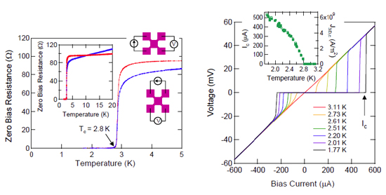
Figure (Left) Temperature dependence of zero bias resistance measured by attaching electrodes to a solid surface substance comprising an indium single atomic layer. The inset shows changes in a wider temperature region. Resistance becomes zero at a temperature of 2.8K. (Right) Bias current–voltage characteristics measured while changing temperature. When the bias current reaches the critical current value (Ic), superconductivity is destroyed and the substance switches to a state having normal resistance. The inset plots Ic and the critical current density (J3D,C) obtained from Ic, as functions of temperature.
If you liked this article, please give it a quick review on ycombinator or StumbleUpon. Thanks

Brian Wang is a Futurist Thought Leader and a popular Science blogger with 1 million readers per month. His blog Nextbigfuture.com is ranked #1 Science News Blog. It covers many disruptive technology and trends including Space, Robotics, Artificial Intelligence, Medicine, Anti-aging Biotechnology, and Nanotechnology.
Known for identifying cutting edge technologies, he is currently a Co-Founder of a startup and fundraiser for high potential early-stage companies. He is the Head of Research for Allocations for deep technology investments and an Angel Investor at Space Angels.
A frequent speaker at corporations, he has been a TEDx speaker, a Singularity University speaker and guest at numerous interviews for radio and podcasts. He is open to public speaking and advising engagements.