
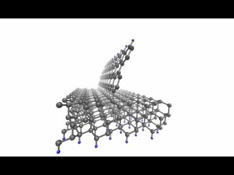
To stand a ribbon of graphene upright, it needs diamond on the soles of its shoes. A new paper by collaborators at Rice University and Hong Kong Polytechnic University demonstrates the possibility that tiny strips of graphene — one-atom-thick sheets of carbon — can stand tall on a substrate with a little support. This leads to the possibility that arrays of graphene walls could become ultrahigh density components of electronic or spintronic devices.
Calculations by Rice theoretical physicist Boris Yakobson, Assistant Professor Feng Ding of Hong Kong Polytechnic and their collaborators showed substrates not only of diamond but also nickel could chemically bind the edge of a strip of a graphene nanoribbon. Because the contact is so slight, the graphene walls retain nearly all of their inherent electrical or magnetic properties.
Journal of the American Chemical Society – Upright Standing Graphene Formation on Substrates
We propose integrating graphene nanoribbons (GNRs) onto a substrate in an upright position whereby they are chemically bound to the substrate at the basal edge. Extensive ab initio calculations show that both nickel (Ni)- and diamond-supported upright GNRs are feasible for synthesis and are mechanically robust. Moreover, the substrate-supported GNRs display electronic and magnetic properties nearly the same as those of free-standing GNRs. Due to the extremely small footprint of an upright GNR on a substrate, standing GNRs are ideal building blocks for synthesis of subnanometer electronic or spintronic devices. Theoretically, standing GNR-based microchips with field-effect transistor (FET) densities up to 10^13 per cm2 are achievable.
Yakobson and Ding calculated a theoretical potential of putting 100 trillion graphene wall field-effect transistors (FETs) on a square-centimeter chip.
That potential alone may make it possible to blow past the limits implied by Moore’s Law — something Yakobson once discussed with Intel founder Gordon Moore himself.
“We met in Montreal, when nano was a new kid on the block, and had a good conversation,” said Yakobson, Rice’s Karl F. Hasselmann Chair in Engineering and a professor of materials science and mechanical engineering and of chemistry. “Moore liked to talk about silicon wafers in terms of real estate. Following his metaphor, an upright architecture would increase the density of circuits on a chip — like going from ranch-style houses in Texas to skyscraper condos in Hong Kong.
“This kind of strategy may help sustain Moore’s Law for an extra decade,” he said.
A sheet of material a fraction of a nanometer wide is pretty pliable, he said, but the laws of physics are on its side. Binding energies between carbon in the diamond matrix and carbon in graphene are maximized at the edge, and the molecules bind strongly at a 90-degree angle. Minimal energy is required for the graphene to stand upright, which is its preferred state. (Walls on a nickel substrate would be angled at about 30 degrees, the researchers found.)
Yakobson said the walls could be as close to each other as 7/10ths of a nanometer, which would maintain the independent electronic properties of individual nanoribbons. They could potentially be grown on silicon, silicon dioxide, aluminum oxide or silicon carbide.
The research illustrated differences between walls made of two distinct types of graphene, zigzag and armchair, so-called because of the way their edges are shaped.
Sheets of graphene are considered semimetals that have limited use in electronics because electrical current shoots straight through without resistance. However, armchair nanoribbons can become semiconductors; the thinner the ribbon, the larger the band gap, which is essential for transistors.
Zigzag nanoribbons are magnetic. Electrons at their opposing edges spin in opposite directions, a characteristic that can be controlled by an electric current; this makes them suitable for spintronic devices.
In both cases, the electronic properties of the walls can be tuned by changing their height.
The researchers also suggested nanowalls could become nanoarches by attaching opposing ends of a graphene ribbon to the substrate. Rather than lie flat on the diamond or nickel surface, the energies at play along the binding edges would naturally force the graphene strip to rise in the middle. It would essentially become a half-nanotube with its own set of potentially useful properties.
Precisely how to turn these two-dimensional building blocks into a three-dimensional device presents challenges, but the payoff is great, Yakobson said. He noted that the research lays the groundwork for subnanometer electronic technology.
5 pages of supplemental information
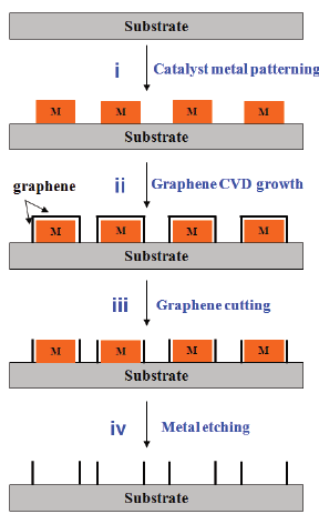
Designed method of synthesizing standing graphene nanoribbons (GNRs)
formation on a substrate: (i) Synthesizing transition metal pattern on a substrate using the lithography technology. (ii) Using the transition metal substrate as catalyst to grow a layer of graphene on the patterned metal surface (iii) Cutting the top part of the patterned metal and grown graphene to achieve desired height by ion beam etching. (iv) Etching away transition metal chemically to achieve the predesigned standing GNR pattern with controlled height for device application.
If you liked this article, please give it a quick review on ycombinator or StumbleUpon. Thanks

Brian Wang is a Futurist Thought Leader and a popular Science blogger with 1 million readers per month. His blog Nextbigfuture.com is ranked #1 Science News Blog. It covers many disruptive technology and trends including Space, Robotics, Artificial Intelligence, Medicine, Anti-aging Biotechnology, and Nanotechnology.
Known for identifying cutting edge technologies, he is currently a Co-Founder of a startup and fundraiser for high potential early-stage companies. He is the Head of Research for Allocations for deep technology investments and an Angel Investor at Space Angels.
A frequent speaker at corporations, he has been a TEDx speaker, a Singularity University speaker and guest at numerous interviews for radio and podcasts. He is open to public speaking and advising engagements.