
National Institute of Standards and Technology (NIST) researchers have a new method for carving diamond crystals. The method offers a precise way to engineer microscopic cuts in a diamond surface, yielding potential benefits in both measurement and technological fields.
NIST semiconductor researchers have found a way to create unique features in diamond—potentially leading to improvements in nanometrology in short order, as it has allowed the team to make holes of precise shape in one of the hardest known substances. But beyond the creation of virtually indestructible nanorulers, the method could one day lead to the improvement of a class of electronic devices useful in cell phones, gyroscopes and medical implants.

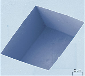
This colorized electron microscope image reveals the boxy shape of the pits the NIST team etched into the diamond surface, exhibiting their smooth vertical sidewalls and flat bottom. The pits were between 1 and 72 micrometers in size.
Credit: NIST
Diamond and Related Materials – Rectangular Scale-Similar Etch Pits in Monocrystalline Diamond
Well known for making the hugely complex electronic microchips that run our laptops, the semiconductor industry has expanded its portfolio by fabricating tiny devices with moving parts. Constructed with substantially the same techniques as the electronic chips, these “micro-electromechanical systems,” or MEMS, are just a few micrometers in size. They can detect environmental changes such as heat, pressure and acceleration, potentially enabling them to form the basis of tiny sensors and actuators for a host of new devices. But designers must take care that tiny moving parts do not grind to a disastrous halt. One way to make the sliding parts last longer without breaking down is to make them from a tougher material than silicon.
“Diamond may be the ideal substance for MEMS devices,” says NIST’s Craig McGray. “It can withstand extreme conditions, plus it’s able to vibrate at the very high frequencies that new consumer electronics demand. But it’s very hard, of course, and there hasn’t been a way to engineer it very precisely at small scales. We think our method can accomplish that.”
The method uses a chemical etching process to create cavities in the diamond surface. The cubic shape of a diamond crystal can be sliced in several ways—a fact jewelers take advantage of when creating facets on gemstones. The speed of the etching process depends on the orientation of the slice, occurring at a far slower rate in the direction of the cube’s “faces”—think of chopping the cube into smaller cubes—and these face planes can be used as a sort of boundary where etching can be made to stop when desired. In their initial experiments, the team created cavities ranging in width from 1 to 72 micrometers, each with smooth vertical sidewalls and a flat bottom.
“We’d like to figure out how to optimize control of this process next,” McGray says, “but some of the ways diamond behaved under the conditions we used were unexpected. We plan to explore some of these mysteries while we develop a prototype diamond MEMS device.”
Etching of monocrystalline diamond in oxygen and water vapor at 1100 °C through small pores in a silicon nitride film produced smooth-walled rectangular cavities. The cavities were imaged by electron microscopy and measured by interferometric microscopy. The observed cavities ranged in width from approximately 1 μm up to 72 μm, in each case exhibiting smooth, vertical sidewalls, a flat bottom, and a depth equal to half its width. Cavity boundaries were determined to lie along slow-etching 100 crystallographic planes, suggesting the possibility of a powerful class of techniques for high-aspect-ratio bulk micromachining of diamond.
If you liked this article, please give it a quick review on ycombinator or StumbleUpon. Thanks

Brian Wang is a Futurist Thought Leader and a popular Science blogger with 1 million readers per month. His blog Nextbigfuture.com is ranked #1 Science News Blog. It covers many disruptive technology and trends including Space, Robotics, Artificial Intelligence, Medicine, Anti-aging Biotechnology, and Nanotechnology.
Known for identifying cutting edge technologies, he is currently a Co-Founder of a startup and fundraiser for high potential early-stage companies. He is the Head of Research for Allocations for deep technology investments and an Angel Investor at Space Angels.
A frequent speaker at corporations, he has been a TEDx speaker, a Singularity University speaker and guest at numerous interviews for radio and podcasts. He is open to public speaking and advising engagements.