

Electronic circuitry composed of nanowires can now be fitted to a surface of almost any shape on an object made of virtually any material, using a new approach to fabrication and transfer of nanowire electronics developed by Stanford researchers.
Stanford researchers have developed a new method of attaching nanowire electronics to the surface of virtually any object, regardless of its shape or what material it is made of. The method could be used in making everything from wearable electronics and flexible computer displays to high-efficiency solar cells and ultrasensitive biosensors.

Photographs of the transferred microelectrode arrays to a range of (a) adhesive substrates such as carbon tape, Kapton tape, double sided tape, Post-it® notes, and (b) nonadhesive substrates such as PDMS and Al foil. (c) Representative SEM images of the transferred microelectrode arrays onto the diverse nonconventional substrates.
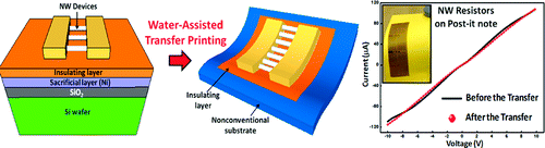
We report a simple, versatile, and wafer-scale water-assisted transfer printing method (WTP) that enables the transfer of nanowire devices onto diverse nonconventional substrates that were not easily accessible before, such as paper, plastics, tapes, glass, polydimethylsiloxane (PDMS), aluminum foil, and ultrathin polymer substrates. The WTP method relies on the phenomenon of water penetrating into the interface between Ni and SiO2. The transfer yield is nearly 100%, and the transferred devices, including NW resistors, diodes, and field effect transistors, maintain their original geometries and electronic properties with high fidelity.
Nanowire electronics are promising building blocks for virtually every digital electronic device used today, including computers, cameras and cell phones. The electronic circuitry is typically fabricated on a silicon chip. The circuitry adheres to the surface of the chip during fabrication and is extremely difficult to detach, so when the circuitry is incorporated into an electronic device, it remains attached to the chip. But silicon chips are rigid and brittle, limiting the possible uses of wearable and flexible nanowire electronics.
The key to the new method is coating the surface of the silicon wafer with a thin layer of nickel before fabricating the electronic circuitry. Nickel and silicon are both hydrophilic, or “water-loving,” meaning when they are exposed to water after fabrication of nanowire devices is finished, the water easily penetrates between the two materials, detaching the nickel and the overlying electronics from the silicon wafer.
“The detachment process can be done at room temperature in water and only takes a few seconds,” said Xiaolin Zheng, an assistant professor of mechanical engineering, who led the research group that developed the process. “The transfer process is almost 100 percent successful, meaning the devices can be transferred without sustaining any damage.”
After detachment, the silicon wafers are clean and ready to reuse, which should reduce manufacturing costs significantly.
After applying the nickel layer to the silicon chip, the researchers also laid down an ultrathin layer of a polymer to act as an insulator and provide mechanical support for the electronics.
The ultrathin polymer layer is also extremely flexible, which is what allows Zheng and her team to attach their nanowire electronics to a wide range of shapes and materials including paper, textiles, plastics, glass, aluminum foil, latex gloves – even a crumpled Coke can and a mashed plastic water bottle.
We report a simple, versatile, and wafer-scale water-assisted transfer printing method (WTP) that enables the transfer of nanowire devices onto diverse nonconventional substrates that were not easily accessible before, such as paper, plastics, tapes, glass, polydimethylsiloxane (PDMS), aluminum foil, and ultrathin polymer substrates. The WTP method relies on the phenomenon of water penetrating into the interface between Ni and SiO2. The transfer yield is nearly 100%, and the transferred devices, including NW resistors, diodes, and field effect transistors, maintain their original geometries and electronic properties with high fidelity.
The transfer process could also be used in developing high-efficiency flexible solar cells and would likely have uses in robotics, as well.
“The possibilities are really unlimited,” Zheng said.
5 pages of supplemental information
If you liked this article, please give it a quick review on ycombinator or StumbleUpon. Thanks

Brian Wang is a Futurist Thought Leader and a popular Science blogger with 1 million readers per month. His blog Nextbigfuture.com is ranked #1 Science News Blog. It covers many disruptive technology and trends including Space, Robotics, Artificial Intelligence, Medicine, Anti-aging Biotechnology, and Nanotechnology.
Known for identifying cutting edge technologies, he is currently a Co-Founder of a startup and fundraiser for high potential early-stage companies. He is the Head of Research for Allocations for deep technology investments and an Angel Investor at Space Angels.
A frequent speaker at corporations, he has been a TEDx speaker, a Singularity University speaker and guest at numerous interviews for radio and podcasts. He is open to public speaking and advising engagements.