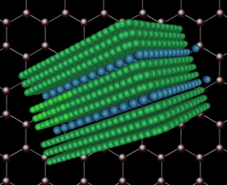
When compounds of bromine or chlorine (represented in blue) are introduced into a block of graphite (shown in green), the atoms find their way into the structure in between every third sheet, thus increasing the spacing between those sheets and making it easier to split them apart. Image: Chih-Jen Shih/Christine Daniloff
A team of MIT scientists has found a way to produce graphene in significant quantities in a two- or three-layer form. When the layers are arranged just right, these structures give graphene the much-desired band gap — an energy range that falls between the bands, or energy levels, where electrons can exist in a given material.
The new method, however, can be carried out at a scale that opens up the possibility of real, practical applications, Strano says, and makes it possible to produce the precise arrangement of the layers — called A-B stacked, with the atoms in one layer centered over the spaces between atoms in the next — that yields desirable electronic properties.
Nature Nanotechnology – Bi- and trilayer graphene solutions
Bilayer and trilayer graphene with controlled stacking is emerging as one of the most promising candidates for post-silicon nanoelectronics. However, it is not yet possible to produce large quantities of bilayer or trilayer graphene with controlled stacking, as is required for many applications. Here, we demonstrate a solution-phase technique for the production of large-area, bilayer or trilayer graphene from graphite, with controlled stacking. The ionic compounds iodine chloride (ICl) or iodine bromide (IBr) intercalate the graphite starting material at every second or third layer, creating second- or third-stage controlled graphite intercolation compounds, respectively. The resulting solution dispersions are specifically enriched with bilayer or trilayer graphene, respectively. Because the process requires only mild sonication, it produces graphene flakes with areas as large as 50 µm2. Moreover, the electronic properties of the flakes are superior to those achieved with other solution-based methods; for example, unannealed samples have resistivities as low as ~1 kΩ and hole mobilities as high as ~400 cm2 V–1 s–1. The solution-based process is expected to allow high-throughput production, functionalization, and the transfer of samples to arbitrary substrates.
Compounds of bromine or chlorine introduced into a block of graphite naturally find their way into the structure of the material, inserting themselves regularly between every other layer, or in some cases every third layer, and pushing the layers slightly farther apart in the process. Strano and his team found that when the graphite is dissolved, it naturally comes apart where the added atoms lie, forming graphene flakes two or three layers thick.
“Because this dispersion process can be very gentle, we end up with much larger flakes” than anyone has made using other methods, Strano says. “Graphene is a very fragile material, so it requires gentle processing.”
Such formations are “one of the most promising candidates for post-silicon nanoelectronics,” the authors say in their paper. The flakes produced by this method, as large as 50 square micrometers in area, are large enough to be useful for electronic applications, they say. To prove the point, they were able to manufacture some simple transistors on the material.
The material can now be used to explore the development of new kinds of electronic and optoelectronic devices, Strano says. And unlike the “Scotch tape” approach to making graphene, “our approach is industrially relevant,” Strano says.
James Tour, a professor of chemistry and of mechanical engineering and materials science at Rice University, who was not involved in this research, says the work involved “brilliant experiments” that produced convincing statistics. He added that further work would be needed to improve the yield of usable graphene material in their solutions, now at about 35 to 40 percent, to more than 90 percent. But once that is achieved, he says, “this solution-phase method could dramatically lower the cost of these unique materials and speed the commercialization of them in applications such as optical electronics and conductive composites.”
While it’s hard to predict how long it will take to develop this method to the point of commercial applications, Strano says, “it’s coming about at a breakneck pace.” A similar solvent-based method for making single-layer graphene is already being used to manufacture some flat-screen television sets, and “this is definitely a big step” toward making bilayer or trilayer devices, he says

18 pages of supplemental material
If you liked this article, please give it a quick review on ycombinator or StumbleUpon. Thanks

Brian Wang is a Futurist Thought Leader and a popular Science blogger with 1 million readers per month. His blog Nextbigfuture.com is ranked #1 Science News Blog. It covers many disruptive technology and trends including Space, Robotics, Artificial Intelligence, Medicine, Anti-aging Biotechnology, and Nanotechnology.
Known for identifying cutting edge technologies, he is currently a Co-Founder of a startup and fundraiser for high potential early-stage companies. He is the Head of Research for Allocations for deep technology investments and an Angel Investor at Space Angels.
A frequent speaker at corporations, he has been a TEDx speaker, a Singularity University speaker and guest at numerous interviews for radio and podcasts. He is open to public speaking and advising engagements.