
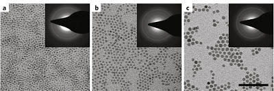
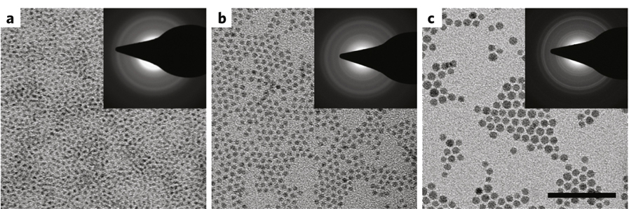
Transmission electron micrographs and (inset) showing the electron diffraction patterns of three quantum dot samples with average size of (a) 2.4 nanometers (b) 3.6 nm, and (c) 5.8 nm. (Image courtesy of Alivisatos group)
With its promise of superfast computers and ultrapowerful optical microscopes among the many possibilities, plasmonics has become one of the hottest fields in high-technology. However, to date plasmonic properties have been limited to nanostructures that feature interfaces between noble metals and dielectrics. Now, researchers with the U.S. Department of Energy (DOE)’s Lawrence Berkeley National Laboratory (Berkeley Lab) have shown that plasmonic properties can also be achieved in the semiconductor nanocrystals known as quantum dots. This discovery should make the field of plasmonics even hotter.

Localized surface plasmon resonance (LSPR) frequency dependence on free carrier density and doping constraints.
“We have demonstrated well-defined localized surface plasmon resonances arising from p-type carriers in vacancy-doped semiconductor quantum dots that should allow for plasmonic sensing and manipulation of solid-state processes in single nanocrystals,” says Berkeley Lab director Paul Alivisatos, a nanochemistry authority who led this research. “Our doped semiconductor quantum dots also open up the possibility of strongly coupling photonic and electronic properties, with implications for light harvesting, nonlinear optics, and quantum information processing.”
Alivisatos is the corresponding author of a paper in the journal Nature Materials titled “Localized surface plasmon resonances arising from free carriers in doped quantum dots.” Co-authoring the paper were Joseph Luther and Prashant Jain, along with Trevor Ewers.
The key to plasmonic properties is when the oscillation frequency between the plasmons and the incident photons matches, a phenomenon known as localized surface plasmon resonance (LSPR). Conventional scientific wisdom has held that LSPRs require a metal nanostructure , where the conduction electrons are not strongly attached to individual atoms or molecules. This has proved not to be the case as Prashant Jain, a member of the Alivisatos research group and one of the lead authors of the Nature Materials paper, explains.
“Our study represents a paradigm shift from metal nanoplasmonics as we’ve shown that, in principle, any nanostructure can exhibit LSPRs so long as the interface has an appreciable number of free charge carriers, either electrons or holes,” Jain says. “By demonstrating LSPRs in doped quantum dots, we’ve extended the range of candidate materials for plasmonics to include semiconductors, and we’ve also merged the field of plasmonic nanostructures, which exhibit tunable photonic properties, with the field of quantum dots, which exhibit tunable electronic properties.”
Jain and his co-authors made their quantum dots from the semiconductor copper sulfide, a material that is known to support numerous copper-deficient stoichiometries. Initially, the copper sulfide nanocrystals were synthesized using a common hot injection method. While this yielded nanocrystals that were intrinsically self-doped with p-type charge carriers, there was no control over the amount of charge vacancies or carriers.
“We were able to overcome this limitation by using a room-temperature ion exchange method to synthesize the copper sulfide nanocrystals,” Jain says. “This freezes the nanocrystals into a relatively vacancy-free state, which we can then dope in a controlled manner using common chemical oxidants.”
By introducing enough free electrical charge carriers via dopants and vacancies, Jain and his colleagues were able to achieve LSPRs in the near-infrared range of the electromagnetic spectrum. The extension of plasmonics to include semiconductors as well as metals offers a number of significant advantages, as Jain explains.
“Unlike a metal, the concentration of free charge carriers in a semiconductor can be actively controlled by doping, temperature, and/or phase transitions,” he says. “Therefore, the frequency and intensity of LSPRs in dopable quantum dots can be dynamically tuned. The LSPRs of a metal, on the other hand, once engineered through a choice of nanostructure parameters, such as shape and size, is permanently locked-in.”
Jain envisions quantum dots as being integrated into a variety of future film and chip-based photonic devices that can be actively switched or controlled, and also being applied to such optical applications as in vivo imaging. In addition, the strong coupling that is possible between photonic and electronic modes in such doped quantum dots holds exciting potential for applications in solar photovoltaics and artificial photosynthesis
“In photovoltaic and artificial photosynthetic systems, light needs to be absorbed and channeled to generate energetic electrons and holes, which can then be used to make electricity or fuel,” Jain says. “To be efficient, it is highly desirable that such systems exhibit an enhanced interaction of light with excitons. This is what a doped quantum dot with an LSPR mode could achieve.”
The potential for strongly coupled electronic and photonic modes in doped quantum dots arises from the fact that semiconductor quantum dots allow for quantized electronic excitations (excitons), while LSPRs serve to strongly localize or confine light of specific frequencies within the quantum dot. The result is an enhanced exciton-light interaction. Since the LSPR frequency can be controlled by changing the doping level, and excitons can be tuned by quantum confinement, it should be possible to engineer doped quantum dots for harvesting the richest frequencies of light in the solar spectrum.
Quantum dot plasmonics also hold intriguing possibilities for future quantum communication and computation devices.
“The use of single photons, in the form of quantized plasmons, would allow quantum systems to send information at nearly the speed of light, compared with the electron speed and resistance in classical systems,” Jain says. “Doped quantum dots by providing strongly coupled quantized excitons and LSPRs and within the same nanostructure could serve as a source of single plasmons.”
Jain and others in Alivsatos’ research group are now investigating the potential of doped quantum dots made from other semiconductors, such as copper selenide and germanium telluride, which also display tunable plasmonic or photonic resonances. Germanium telluride is of particular interest because it has phase change properties that are useful for memory storage devices.
“A long term goal is to generalize plasmonic phenomena to all doped quantum dots, whether heavily self-doped or extrinsically doped with relatively few impurities or vacancies,” Jain says.
3 pages of supplemental information
If you liked this article, please give it a quick review on ycombinator or StumbleUpon. Thanks

Brian Wang is a Futurist Thought Leader and a popular Science blogger with 1 million readers per month. His blog Nextbigfuture.com is ranked #1 Science News Blog. It covers many disruptive technology and trends including Space, Robotics, Artificial Intelligence, Medicine, Anti-aging Biotechnology, and Nanotechnology.
Known for identifying cutting edge technologies, he is currently a Co-Founder of a startup and fundraiser for high potential early-stage companies. He is the Head of Research for Allocations for deep technology investments and an Angel Investor at Space Angels.
A frequent speaker at corporations, he has been a TEDx speaker, a Singularity University speaker and guest at numerous interviews for radio and podcasts. He is open to public speaking and advising engagements.