

Commercial MRAMs have been on the market since 2005. They are, however, still slower than the competitors they have among the volatile storage media. Physikalisch-Technische Bundesanstalt (PTB) has a new special chip connection, in association with dynamic triggering of the component, reduces the response from – so far – 2 ns to below 500 ps. This corresponds to a data rate of up to 2 GBit (instead of the approx. 400 MBit so far). Power consumption and the thermal load will be reduced, as well as the bit error rate.
MRAMs are potentially universal storage chips because they allow – in addition to the non-volatile information storage – also faster access, a high integration density and an unlimited number of writing and reading cycles. However, the current MRAM models are not yet fast enough to outperform the best competitors.
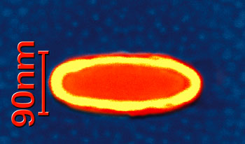
PTB scientists have optimized the MRAM design and integrated the so-called ballistic bit triggering which has also been developed at PTB. Here, the magnetic pulses which serve for the programming are selected in such a skilful way that the other cells in the MRAM are hardly magnetically excited at all. The pulse ensures that the magnetization of a cell which is to be switched performs half a precision rotation (180°), while a cell whose storage state is to remain unchanged performs a complete precision rotation (360°). In both cases, the magnetization is in the state of equilibrium after the magnetic pulse has decayed, and magnetic excitations do not occur any more.
This optimal bit triggering also works with ultra-short switching pulses with a duration below 500 ps. The maximum clock rates of the MRAM are, therefore, above 2 GHz. In addition, several bits can be programmed at the same time which would allow the effective write rate per bit to be increased again by more than one order. This invention allows clock rates to be achieved with MRAM which can compete with those of the fastest volatile storage components.
If you liked this article, please give it a quick review on ycombinator or StumbleUpon. Thanks

Brian Wang is a Futurist Thought Leader and a popular Science blogger with 1 million readers per month. His blog Nextbigfuture.com is ranked #1 Science News Blog. It covers many disruptive technology and trends including Space, Robotics, Artificial Intelligence, Medicine, Anti-aging Biotechnology, and Nanotechnology.
Known for identifying cutting edge technologies, he is currently a Co-Founder of a startup and fundraiser for high potential early-stage companies. He is the Head of Research for Allocations for deep technology investments and an Angel Investor at Space Angels.
A frequent speaker at corporations, he has been a TEDx speaker, a Singularity University speaker and guest at numerous interviews for radio and podcasts. He is open to public speaking and advising engagements.