


IEEE Computer – From Microprocessors to Nanostores: Rethinking Data-Centric Systems
Historically, the first computer to achieve terascale computing (10^12, or one trillion operations per second) was demonstrated in the late 1990s. In the 2000s, the first petascale computer was demonstrated with a thousand-times better performance. Extrapolating these trends, we can expect the first exascale computer (with one million trillion operations per second) to appear around the end of this next decade.
Emerging technologies such as photonics, nonvolatile memory, 3D stacking, and new datacentric workloads offer compelling new opportunities. The confluence of these trends motivates a rethinking of the basic systems’ building blocks of the future and a likely new design approach called nanostores that focus on data-centric workloads and hardware-software codesign for upcoming technologies.
HP Data Central blog provides an overview of the memristor work.
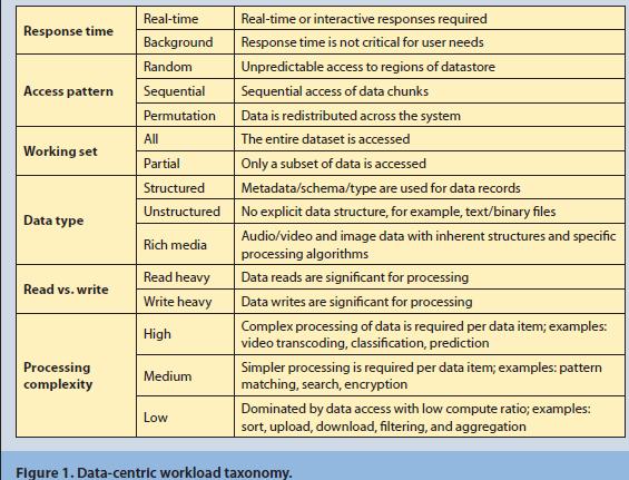
Compared to traditional enterprise workloads such as online transaction processing and Web services, emerging data-centric workloads change many assumptions about system design. These workloads typically operate at larger scale (hundreds of thousands of servers) and on more diverse data (structured, unstructured, rich media) with I/O-intensive, often random, data access patterns and limited locality. In addition, these workloads are characterized by innovations in the software stack targeted at increased scalability and commodity hardware such as Google’s MapReduce and BigTable.

More details about emerging nonvolatile memories can be found in several recent overviews and tutorials 14,15—for example, HotChips 2010 (www.hotchips.org).
Nanostores: A New System Architecture Building Block?
The confluence of these various trends—future largescale distributed data-centric workloads with I/O-intensive behavior, innovations in the software stack, and the emergence of new nonvolatile memories potentially timed with the end of scaling for DRAM—offers a unique opportunity to rethink traditional system architectures and memory hierarchies in future designs.
Nanostores offer one such intuitive, and potentially advantageous, way to leverage this confluence of application and technology trends. We coined the term nanostores as a duality of microprocessors to reflect the evolution to nanotechnology and the emphasis on data instead of compute. The key property of nanostores is the colocation of processors with nonvolatile storage, eliminating many intervening levels of the storage hierarchy. All data is stored in a single-level nonvolatile memory datastore that replaces traditional disk and DRAM layers—disk use is relegated to archival backups.
For example, a single nanostore chip consists of multiple 3D-stacked layers of dense silicon nonvolatile memories such as PCMs or memristors, with a top layer of power-efficient compute cores. Through-silicon vias are used to provide wide, low-energy datapaths between the processors and the datastores. Each nanostore can act as a full-fledged system with a network interface. Individual such nanostores are networked through onboard connectors to form a large-scale distributed system or cluster akin to current large-scale clusters for data-centric computing. The system can support different network topologies, including traditional fat trees or recent proposals like HyperX.
In terms of physical organization, multiple nanostore chips are organized into small daughter boards (microblades) that, in turn, plug into traditional blade server boards. Given the heat dissipation characteristics of the design, we also can envision newer packaging technologies for the broader solution. The first figure of this article illustrates an example dematerialized datacenter design in which the individual blade servers connect to an optical backplane “spine” with optimized airflow and packaging density.
Current flash memories are about an order of magnitude more costly on a dollar-per-byte basis compared to disk. NVRAM has the potential to lower these costs by allowing more aggressive stacking and simpler fabrication processes. The improved energy efficiency of nanostores can also further lower total costs of ownership. Based on these observations, we expect the nanostore design to be competitive in costs compared to traditional designs, but this needs to be validated with further study.
The Hot Chips panel supports Dr. Ranganathan’s memory-centric approach. It found that the energy cost of a single calculation was about 70 picojoules (a picojoule is one millionth of one millionth of a joule. The energy needed to keep a 100-watt bulb lit for an hour is 360,000 joules). However, when the energy costs of moving the data needed to do a single calculation — moving 200 bits of data in and out of memory multiple times — the real energy cost of a single calculation might be anywhere from 1,000 to 10,000 picojoules.
A range of other technologies are being explored to allow the continued growth of computing power, including ways to build electronic switches smaller than 10 nanometers — thought to be the minimum size for current chip-making techniques.
Last month, for example, researchers at Harvard and Mitre Corporation reported the development of nanoprocessor “tiles” based on electronic switches fabricated from ultrathin germanium-silicon wires.
I.B.M. researchers have been pursuing so-called phase-change memories based on the ability to use an electric current to switch a material from a crystalline to an amorphous state and back again. This technology was commercialized by Samsung last year. More recently, I.B.M. researchers have said that they are excited about the possibility of using carbon nanotubes as an a partial step to build hybrid systems that straddle the nanoelectronic and microelectronic worlds.
If you liked this article, please give it a quick review on ycombinator or StumbleUpon. Thanks

Brian Wang is a Futurist Thought Leader and a popular Science blogger with 1 million readers per month. His blog Nextbigfuture.com is ranked #1 Science News Blog. It covers many disruptive technology and trends including Space, Robotics, Artificial Intelligence, Medicine, Anti-aging Biotechnology, and Nanotechnology.
Known for identifying cutting edge technologies, he is currently a Co-Founder of a startup and fundraiser for high potential early-stage companies. He is the Head of Research for Allocations for deep technology investments and an Angel Investor at Space Angels.
A frequent speaker at corporations, he has been a TEDx speaker, a Singularity University speaker and guest at numerous interviews for radio and podcasts. He is open to public speaking and advising engagements.