

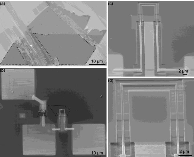
Scanning electron micrographs showing: (a) The graphene flake. The dashed outline marks the areas suitable for formation of the devices; (b) The device and the contact pads, with the dashed outline marking the same area as in (a); (c) the graphene U-shaped device with tungsten contact wires and pads, (d) detail of the graphene U-shaped device.
Arxiv – A U-shaped bilayer graphene channel transistor with a very high I on /I off ratio (8 pages) I is current. I on is current flowing and I off is the zero current state.
A novel graphene transistor architecture is reported. The transistor has a U-shape geometry and was fabricated using a gallium focused ion beam (FIB). The channel conductance was tuned with a back gate. The I on /I off ratio exceeded 100,000. Previously the best I on / I off ratio was less than 100.
Zakaria Moktadir and others at the Nano Research Group at the University of Southampton, UK created this latest improvement.
The difference between these two states is called the current on/off ratio, and graphene’s low on/off ratio has long been a major barrier to using it in transistors for logic gates and ultimately computer chips.
A low on/off ratio means that the processor would have to use more power, and so would be less efficient.
The problem can be overcome by using either a strong electric field to switch the transistor or by making the transistors out of extremely narrow ribbons of graphene, just a few nanometres wide. But large electric fields require large voltages, and it’s difficult to make nanoribbons narrower than 5 nanometres with any degree of accuracy.
But Moktadir reckons he has discovered a third way to get graphene switching more efficiently. By making a normally flat transistor similar to a U-shape, but with corners instead of a curve at the bottom, he has found that he can switch it off entirely, increasing the current on/off ratio thousandfold. “We are still trying to explain why it’s happening, but we attribute it to the corners,” he says.
Working with graphene just a few hundred nanometres wide, sharp corners are known to produce unusual behaviour, says Moktadir. But making such corners is challenging because conventional electron-beam lithography – using electrons to create a circuit on a nanometre scale – leaves corners somewhat rounded.
Moktadir and colleagues got round this by using a gallium focused ion beam to create U-shaped ribbons of graphene 300 nanometres wide and a few micrometres long. Reporting their findings in Electronics Letters, Moktadir says this new approach overcomes the issue.
If you liked this article, please give it a quick review on ycombinator or StumbleUpon. Thanks

Brian Wang is a Futurist Thought Leader and a popular Science blogger with 1 million readers per month. His blog Nextbigfuture.com is ranked #1 Science News Blog. It covers many disruptive technology and trends including Space, Robotics, Artificial Intelligence, Medicine, Anti-aging Biotechnology, and Nanotechnology.
Known for identifying cutting edge technologies, he is currently a Co-Founder of a startup and fundraiser for high potential early-stage companies. He is the Head of Research for Allocations for deep technology investments and an Angel Investor at Space Angels.
A frequent speaker at corporations, he has been a TEDx speaker, a Singularity University speaker and guest at numerous interviews for radio and podcasts. He is open to public speaking and advising engagements.