

Hard-tip, soft-spring lithography (HSL) rolls into one method the best of scanning-probe lithography — high resolution — and the best of polymer pen lithography — low cost and easy implementation.
HSL could be used in the areas of electronics (electronic circuits), medical diagnostics (gene chips and arrays of biomolecules) and pharmaceuticals (arrays for screening drug candidates), among others.
Nature – Hard-tip, soft-spring lithography

The pyramid on the dollar made only tens of microns across
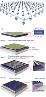
Schematic illustration of an HSL tip array supported by a transparent, soft backing layer that provides mechanical flexibility to each tip. b, Experimental procedure to fabricate the tip arrays: 50-μm-thick (100)Si wafers with thermally
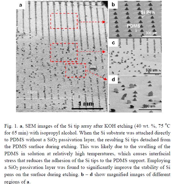
Nanofabrication strategies are becoming increasingly expensive and equipment-intensive, and consequently less accessible to researchers. As an alternative, scanning probe lithography has become a popular means of preparing nanoscale structures, in part owing to its relatively low cost and high resolution, and a registration accuracy that exceeds most existing technologies. However, increasing the throughput of cantilever-based scanning probe systems while maintaining their resolution and registration advantages has from the outset been a significant challenge. Even with impressive recent advances in cantilever array design, such arrays tend to be highly specialized for a given application, expensive, and often difficult to implement. It is therefore difficult to imagine commercially viable production methods based on scanning probe systems that rely on conventional cantilevers. Here we describe a low-cost and scalable cantilever-free tip-based nanopatterning method that uses an array of hard silicon tips mounted onto an elastomeric backing. This method—which we term hard-tip, soft-spring lithography—overcomes the throughput problems of cantilever-based scanning probe systems and the resolution limits imposed by the use of elastomeric stamps and tips: it is capable of delivering materials or energy to a surface to create arbitrary patterns of features with sub-50-nm resolution over centimetre-scale areas. We argue that hard-tip, soft-spring lithography is a versatile nanolithography strategy that should be widely adopted by academic and industrial researchers for rapid prototyping applications.
To demonstrate the method’s capabilities, the researchers duplicated the pyramid on the U.S. one-dollar bill and the surrounding words approximately 19,000 times at 855 million dots per square inch. Each image consists of 6,982 dots. (They reproduced a bitmap representation of the pyramid, including the “Eye of Providence.”) This exercise highlights the sub-50-nanometer resolution and the scalability of the method.
Hard-tip, soft-spring lithography is to scanning-probe lithography what the disposable razor is to the razor industry,” said Chad A. Mirkin, the paper’s senior author. “This is a major step forward in the realization of desktop fabrication that will allow researchers in academia and industry to create and study nanostructure prototypes on the fly.”
Mirkin is the George B. Rathmann Professor of Chemistry in the Weinberg College of Arts and Sciences and professor of medicine, chemical and biological engineering, biomedical engineering and materials science and engineering and director of Northwestern’s International Institute for Nanotechnology.
Micro- and nanolithographic techniques are used to create patterns and build surface architectures of materials on a small scale.
Scanning probe lithography, with its high resolution and registration accuracy, currently is a popular method for building nanostructures. The method is, however, difficult to scale up and produce multiple copies of a device or structure at low cost.
Scanning probe lithographies typically rely on the use of cantilevers as the printing device components. Cantilevers are microscopic levers with tips, typically used to deposit materials on surfaces in a printing experiment. They are fragile, expensive, cumbersome and difficult to implement in an array-based experiment.
“Scaling cantilever-based architectures at low cost is not trivial and often leads to devices that are difficult to operate and limited with respect to the scope of application,” Mirkin said.
Hard-tip, soft-spring lithography uses a soft polymer backing that supports sharp silicon tips as its “print head.” The spring polymer backing allows all of the tips to come in contact with the surface in a uniform manner and eliminates the need to use cantilevers. Essentially, hard tips are floating on soft polymeric springs, allowing either materials or energy to be delivered to a surface.
HSL offers a method that quickly and inexpensively produces patterns of high quality and with high resolution and density. The prototype arrays containing 4,750 tips can be fabricated for the cost of a single cantilever-based tip and made in mass, Mirkin said.
Mirkin and his team demonstrated an array of 4,750 ultra-sharp silicon tips aligned over an area of one square centimeter, with larger arrays possible. Patterns of features with sub-50-nanometer resolution can be made with feature size controlled by tip contact time with the substrate.
They produced patterns “writing” with molecules and showed that as the tips push against the substrate the flexible backing compresses, indicating the tips are in contact with the surface and writing is occurring. (The silicon tips do not deform under pressure.)
“Eventually we should be able to build arrays with millions of pens, where each pen is independently actuated,” Mirkin said.
8 pages of supplemental material
If you liked this article, please give it a quick review on ycombinator or StumbleUpon. Thanks

Brian Wang is a Futurist Thought Leader and a popular Science blogger with 1 million readers per month. His blog Nextbigfuture.com is ranked #1 Science News Blog. It covers many disruptive technology and trends including Space, Robotics, Artificial Intelligence, Medicine, Anti-aging Biotechnology, and Nanotechnology.
Known for identifying cutting edge technologies, he is currently a Co-Founder of a startup and fundraiser for high potential early-stage companies. He is the Head of Research for Allocations for deep technology investments and an Angel Investor at Space Angels.
A frequent speaker at corporations, he has been a TEDx speaker, a Singularity University speaker and guest at numerous interviews for radio and podcasts. He is open to public speaking and advising engagements.