

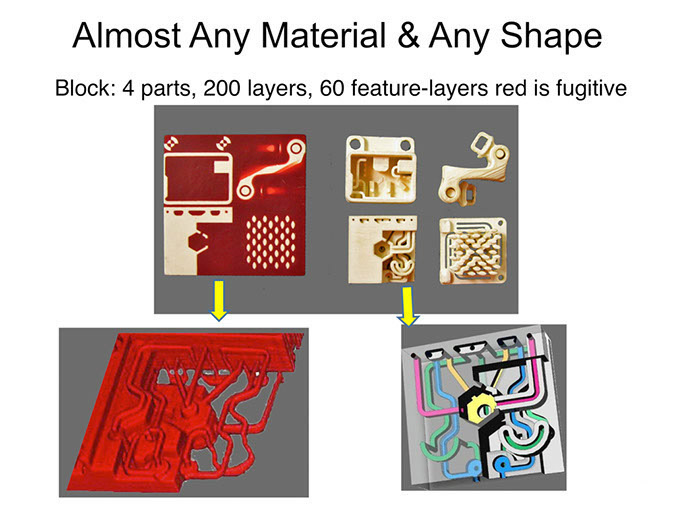
Eoplex Technologies has unique 3D Printing manufacturing capabilities.
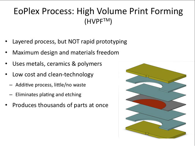
IEEE Spectrum – A California startup, Eoplex has come up with a combination of secret sauces and manufacturing techniques that lets it print sub-micron size voxels of stuff to mass produce 3D objects. After some simple, but secret, processing this stuff turns into metal, ceramics, and empty spaces. The result can be miniature machines with moving parts, metamaterials-enabled multi-function antennas, piezoelectric powered energy harvesters, coin-sized hydrogen fuel cells, pretty much anything.
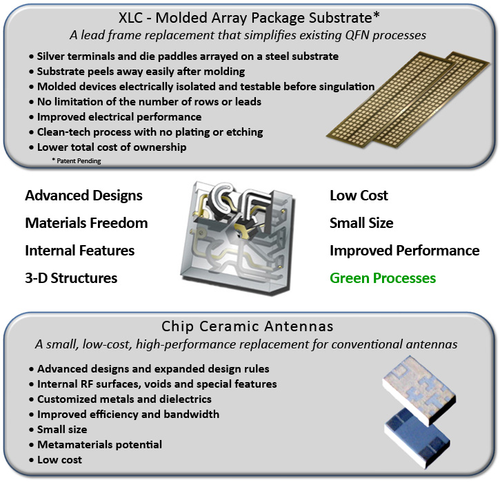
There’s a type of chip packaging called QFN (for Quad Flat No leads) that’s all the rage for packaging chips for mobile devices. The key to QFNs are the lead-frames, delicate spider-works of metal laid out by the dozens on a rather expensive tape. The lead frames are made by etching away a film of metal from the tape, using various nasty chemicals. What you’re left with is a set of leads that look like q-tips surrounding a central slab of metal that conducts heat away from the chip. The long end of the q-tip is just to anchor it to the frame; it doesn’t have an electrical purpose. In the packaging process the chips are stuck to the lead frame, and delicate wires are connected between the chip and the leads on the tape. That familiar black plastic is then flowed over the chip, and then the frame, chip, and plastic are peeled from the tape. Finally, the packaged chips are diced up, tested, and shipped.
The ideal QFN package would not be made using a chemical etch (so it’s a relatively green process), have no extra metal (so it would have better electrical performance, so chips could be tested before dicing, and so dicing would be quicker), as many rows of leads as you want (so you could get data on and off the chip faster), and no tape (so it would be cheaper).
Instead of starting with a film of metal on tape, Eoplex prints a layer of recyclable steel alloy and then tops it with the electrically important parts of the leads (the tip, not the stick) and the thermal pad—both made of silver.
Eoplex has its sights on about $700 million worth of the QFN market, which could grow to $1.3 billion by 2014. By then, he says, the process might be used in other packaging forms such as ball grid array, meaning a $4 billion market.
They discovered the secret voxel pattern that’s key to the QFN product by accident. And, according to Chait, that might be good for keeping competitors at bay
5 page white paper, A High Performance and Cost Effective Molded Array Package Substrate
This White Paper discusses a new packaging family that combines the manufacturing efficiencies of QFN with greater design flexibility and performance than BGAs and QFPs. In addition, the molded array package (MAP) substrate simplifies assembly flow and enables test in the strip prior to singulation. EoPlex’s unique print forming processes and advanced materials combine to create a MAP substrate that is more cost effective and is also very environmentally friendly in both its manufacture and use
It is very desirable to develop a substrate to replace the QFN type leadframe for Molded Array Packages. A substrate provides a removable carrier for the package terminals, power and ground rings, and die pad(s), eliminating the electrical and mechanical interconnection of package components after the carrier is removed. Substrates allowing for removal of the carrier after molding by etching it away and by peeling it off have been advanced but are not ideal, being limited primarily because of cost. EoPlex Technologies has developed a substrate with a peelable carrier that is manufactured by a proprietary printing process that promises to significantly reduce substrate cost while maintaining all of the desirable features of a molded array package substrate
.
If you liked this article, please give it a quick review on ycombinator or StumbleUpon. Thanks
Featured articles
Ocean Floor Gold and Copper
Ocean Floor Mining Company

Brian Wang is a Futurist Thought Leader and a popular Science blogger with 1 million readers per month. His blog Nextbigfuture.com is ranked #1 Science News Blog. It covers many disruptive technology and trends including Space, Robotics, Artificial Intelligence, Medicine, Anti-aging Biotechnology, and Nanotechnology.
Known for identifying cutting edge technologies, he is currently a Co-Founder of a startup and fundraiser for high potential early-stage companies. He is the Head of Research for Allocations for deep technology investments and an Angel Investor at Space Angels.
A frequent speaker at corporations, he has been a TEDx speaker, a Singularity University speaker and guest at numerous interviews for radio and podcasts. He is open to public speaking and advising engagements.