
Ad Support : Nano Technology Netbook Technology News Computer Software
Here is the Boris Yakobson interview by Sander Olson. Dr. Yakobson is a materials science professor at Rice University, which was the University which initially discovered buckyballs and had key discoveries in the development of buckytubes and nanotubes. Dr. Yakobson has done groundbreaking research on both graphene and graphane, which is graphene modified by hydrogen atoms. Graphene and graphane have considerable potential in structural materials, as future electronic devices, nanosensors, long distance, high-efficiency power lines, and hydrogen storage mediums. Dr. Yakobson already has several patents related to making heterojunction transistors out of carbon nanotubes.
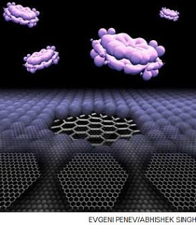
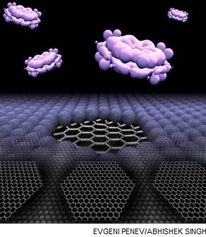
Dr. Yakobson graphane work was covered here in May
Zyvex Performance Materials describes many existing products that use carbon nanotubes.
Question: Your research lab has recently made a breakthrough with graphane.
Answer: Through computational modeling, we have found very interesting physical properties in hybrid structures of graphEne, which consists of a one atom thick sheet of carbon, with graphAne, which is hydrogenated graphene. Graphane is an insulator, so the hybrid in two dimensions has tunable electronic properties. Since this material can be assembled in a variety of desirable ways, it opens up possibilities for utility as quantum dots, interconnects, and their further architectures.
Question: How would these carbon dots be created?
Answer: We have explored – so far, computationally and theoretically — the feasibility of using some chemistry to make such quantum dots. These quantum dots can be formed by attaching hydrogen to pure graphene carbon. Alternately one could start with graphane (already graphene with the hydrogen) and remove H from selected areas. Either way can lead to success but needs significant work yet.
Question: It sounds like graphane could be also used for hydrogen storage.
Answer: Yes, this material consists of about 8% of hydrogen, and could prove ideal as the hydrogen storage media, if kinetics permits. There are catalytic paths, so it could make for a high-efficiency energy storage system. Ideally a hydrogen storage mechanism would operate at room temperature at atmospheric pressures. Carbon is one of the lighter elements and it has a lot of surface area to adsorb hydrogen. 8% of its weight in hydrogen would actually exceed the DOE target numbers.
Question: When will the first integrated circuit made from graphene be demonstrated?
Answer: Hard to tell, I think we are still answering to “if” before one can reasonably speculate on “when”. There has already been progress on that front reported in labs. In a couple of years we should see reasonably defined quantum dots in labs, and hopefully from there it will be scaled up to large-scale production. But we aren’t sure that hydrogen is the optimal material for quantum dots – fluorine, hydroxyl, or some other functional groups might prove superior.
Question: Is a graphene integrated circuit within five years feasible?
Answer: “It’s tough to make predictions, especially about the future” (Yogi Berra). Yet I would like to believe it is feasible, to see a graphene IC elements created in research labs within two-three years. Another three years after that it could go into production.
Question: Your lab has also done extensive investigations into carbon nanotubes. How quickly will the cost of nanotubes decline?
Answer: It has already declined significantly. Further answer really depends on the chirality of nanotubes, that is if one cares or not about it being specific. The key is to control chirality, and our lab has worked on that issue. Current nanotube production methods result in a mixture of semiconducting and metallic nanotubes. Our lab has been working on the origins of chirality hoping to then derive methods to control it, which would be a major step forward. It would allow us to grow separate and distinct batches of semiconducting and metallic nanotubes. We hope for better understanding or maybe a breakthrough within a year. Although this has so far proven to be very elusive.
Question: At what point will it be cost-effective to embed nanotubes in materials?
Answer: The first materials that are embedded with nanotubes are starting to become available for specialized applications such as aerospace. For more cost-sensitive applications, such as roofing or tires, the cost will need to come down considerably, so this may never happen. When the technology is mature I could even see it being used for applications like space elevators. I do not work on it but there is a sustained community of enthusiasts, with annual international meetings, debates, proposals; it ignites young imagination which is a great thing.
Question: Besides quantum dots, structural materials, and energy storage, what else could nanotubes be used for?
Answer: Chemical and bio sensors are a definite possibility. Field emission elements in displays are another potential application, since nanotubes could facilitate the production of large, high-resolution displays.
Question: What about nanotube transistors?
Answer: Many labs are working on that. Nanotubes can be used to make transistors that operate in the very high frequency range. At this point no one knows how long conventional silicon scaling will last. But we may see silicon valley evolve into carbon valley.
Question: Who is funding your lab?
Answer: We are funded both by Federal agencies and some private sources. The Department of Energy, the National Science Foundation, the Office of Naval Research, and the Air Force. We have received funding from Lockheed Martin Corp. and The Welch Foundation. We are also in negotiations with a potentially large private investor.
Question: Do you have any plans to form any startups?
Answer: I have thought about forming a startup, but I currently don’t have the time. If I were to form a startup I would want to partner with someone who understands both the technical-experimental and business aspects. I have a patent on making heterojunction transistors out of nanotubes, so if I were to found a startup it would probably be in that area, there are also 2-3 patents pending in closely related areas. I would more likely encourage my students to consider startups.
Question: Could carbon nanotubes be used to make power lines?
Answer: We have worked on that issue with my colleagues at Rice. There are many challenges, most notably how to create long enough nanotubes. But if we found a way to create nanotubes of arbitrary length and preferable conducting type, we could fabricate nanotube power cables that would be light, heat resistant, and have a very high thermal conductivity. Nanotubes could form the basis of extremely efficient power lines.
If you liked this article, please give it a quick review on Reddit, or StumbleUpon. Thanks
Supporting Advertising
Business Success
How to Make Money
Executive Jobs
Paid Surveys
Thank You

Brian Wang is a Futurist Thought Leader and a popular Science blogger with 1 million readers per month. His blog Nextbigfuture.com is ranked #1 Science News Blog. It covers many disruptive technology and trends including Space, Robotics, Artificial Intelligence, Medicine, Anti-aging Biotechnology, and Nanotechnology.
Known for identifying cutting edge technologies, he is currently a Co-Founder of a startup and fundraiser for high potential early-stage companies. He is the Head of Research for Allocations for deep technology investments and an Angel Investor at Space Angels.
A frequent speaker at corporations, he has been a TEDx speaker, a Singularity University speaker and guest at numerous interviews for radio and podcasts. He is open to public speaking and advising engagements.