

Ad Support : Nano Technology Netbook Technology News Computer Software
Quantum dot laser featuring an active layer containing high-density arrays of quantum dots
Fujitsu Limited, Fujitsu Laboratories Ltd., and the University of Tokyo today announced the world’s first quantum dot laser-based 25 Gbps high-speed data transmission.
Quantum dot lasers are a type of laser being anticipated as a next-generation semiconductor laser capable of handling high-speed data transmissions while consuming minimal power. As increasing the number of quantum dots is known to improve a quantum dot laser’s operation speed, layers of quantum dots with a higher density than conventionally employed were stacked, thereby doubling the laser’s operation speed and enabling a significant improvement over previous technologies. This new technology is expected to be employed for optical sources for next-generation high-speed data communications that aim to achieve data transmission speeds of 100 Gbps, ten times faster than current data transmission speeds.
Quantum well lasers, which have conventionally been used as optical sources for data communications, have a problem of dramatic increases in power consumption attributable to increased driving current when temperatures rise. The quantum dot laser developed by Fujitsu Laboratories and the University of Tokyo uses 3-dimensional (3D) semiconductor nanostructures to produce quantum effects, thus giving it excellent characteristics, including stable operation over a range of temperatures and low power consumption. However, the quantum dot laser had been limited to handling data transfer speeds up to 10 Gbps.
Overview of Newly-developed Technology In order to increase the speed of quantum dot lasers, it was necessary to increase the laser’s optical gain, which in turn required an increase in the number of underlying quantum dots. New quantum dot fabrication technology was developed and applied, resulting in a quantum dot laser capable of high-speed operations at 25 Gbps.
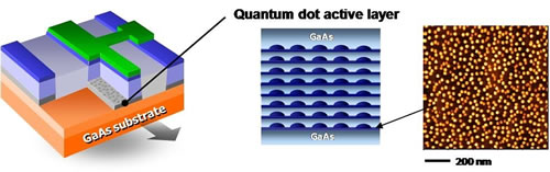
Key features of the newly-developed technologies are as follows (Figure 1):
1. A technology for forming high-density indium-arsenide (InAs) quantum dots on the surface of a gallium-arsenide (GaAs) substrate. This doubles the number of quantum dots per unit area to 6 x 10¹⁰ per 1cm2.
2. A technology for stacking multiple layers of high-density quantum dots. This increases the number of possible layers to 8 layers, an increase from the previously-available 5 layers.
Quantum dots are fabricated using molecular beams in a high-vacuum chamber to embed indium (In) and arsenide (As) in GaAs . Because the atomic distance in InAs is greater than in GaAs, strain is induced in the InAs crystallized on the GaAs substrate. The strain energy can be relaxed by forming 3D crystals, in which each 3D nanocrystal functions as a single quantum dot.
By optimizing the growth conditions in which the 3D crystals are formed, a technology has been developed to double the in-plane area density of the quantum dots to 6 x 10^10 per 1cm^2. Technology was also developed that allows 8 layers – instead of 5 layers – to be stacked while preserving the same high-density in-plane.
Fabrication of quantum dots by employing these aforementioned technologies enabled an increase in number of quantum dots, thereby increasing the optical gain. As a world first, a quantum dot laser employing this active layer was successfully tested at 25 Gbps high-speed modulation.
If you liked this article, please give it a quick review on Reddit, or StumbleUpon. Thanks
Supporting Advertising
Business Success
How to Make Money
Executive Jobs
Paid Surveys
Thank You

Brian Wang is a Futurist Thought Leader and a popular Science blogger with 1 million readers per month. His blog Nextbigfuture.com is ranked #1 Science News Blog. It covers many disruptive technology and trends including Space, Robotics, Artificial Intelligence, Medicine, Anti-aging Biotechnology, and Nanotechnology.
Known for identifying cutting edge technologies, he is currently a Co-Founder of a startup and fundraiser for high potential early-stage companies. He is the Head of Research for Allocations for deep technology investments and an Angel Investor at Space Angels.
A frequent speaker at corporations, he has been a TEDx speaker, a Singularity University speaker and guest at numerous interviews for radio and podcasts. He is open to public speaking and advising engagements.