

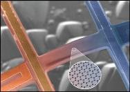
A one-atom thick sheet of graphene (highlighted in the circular window) on top of a silicon dioxide support proves to be an excellent thermal conductor, according to new research published in the journal Science. Although the interaction with the silicon dioxide suppressed the thermal conductivity of graphene compared to its freestanding form, supported graphene still demonstrated much higher heat conducting capability than silicon and copper nanostructures. This finding combined with graphene’s superior strength and electron mobility make it a promising candidate for use in next-generation nano-electronic devices.
1. When suspended, graphene has extremely high thermal conductivity of 3,000 to 5,000 watts per meter per Kelvin. But for practical applications, the chicken-wire like graphene lattice would be attached to a substrate. Boston College Researchers found supported graphene still has thermal conductivity as high as 600 watts per meter per Kelvin near room temperature. That far exceeds the thermal conductivities of copper, approximately 250 watts, and silicon, only 10 watts, thin films currently used in electronic devices.
2. Following up on graphene films clearing a major hurdle to production
They have successfully used direct chemical vapor deposition (CVD) to synthesize single-layer films of graphene on a dielectric substrate. This is exciting news for electronic applications because chemical vapor deposition is a technique already widely used in the semiconductor industry.
A combination of scanning Raman mapping and spectroscopy, plus scanning electron and atomic force microscopy confirmed the presence of continuous single-layer graphene films coating metal-free areas of dielectric substrate measuring tens of square micrometers.
“Further improvement on the control of the dewetting and evaporation process could lead to the direct deposition of patterned graphene for large-scale electronic device fabrication, Zhang says. “This method could also be generalized and used to deposit other two-dimensional materials, such as boron-nitride.”
Even the appearance of wrinkles in the graphene films that followed along the lines of the dewetting shape of the copper could prove to be beneficial in the long-run. Although previous studies have indicated that wrinkles in a graphene film have a negative impact on electronic properties by introducing strains that reduce electron mobility, Zhang believes the wrinkles can be turned to an advantage.
“If we can learn to control the formation of wrinkles in our films, we should be able to modulate the resulting strain and thereby tailor electronic properties,” he says.
“Further study of the wrinkle formation could also give us important new clues for the formation of graphene nanoribbons.”
If you liked this article, please give it a quick review on Reddit, or StumbleUpon. Thanks
Supporting Advertising
Trading Futures Nano Technology Netbook Technology News Computer SoftwareFuture Predictions
Thank You

Brian Wang is a Futurist Thought Leader and a popular Science blogger with 1 million readers per month. His blog Nextbigfuture.com is ranked #1 Science News Blog. It covers many disruptive technology and trends including Space, Robotics, Artificial Intelligence, Medicine, Anti-aging Biotechnology, and Nanotechnology.
Known for identifying cutting edge technologies, he is currently a Co-Founder of a startup and fundraiser for high potential early-stage companies. He is the Head of Research for Allocations for deep technology investments and an Angel Investor at Space Angels.
A frequent speaker at corporations, he has been a TEDx speaker, a Singularity University speaker and guest at numerous interviews for radio and podcasts. He is open to public speaking and advising engagements.