

Ad Support : Nano Technology Netbook Technology News Computer Software
Charles S. Taylor, the grandson of Boston Globe publisher Charles H. Taylor, developed manufacturing technology in which converted commercial printing equipment produces tiny layers of materials that stack up to produce complex designs with multiple functions.
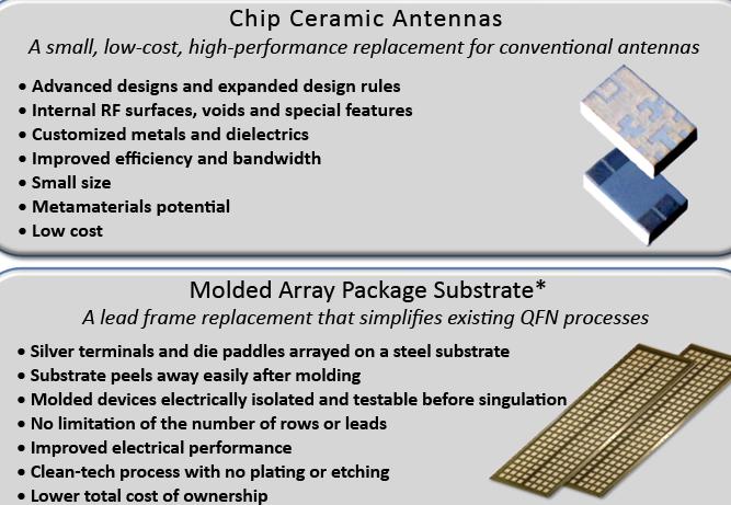
That technology is now in the final qualification stage for antennas used in cell phones and is on the verge of becoming a major player in IC packages for portable electronics. Other potential applications include fluidic parts, energy harvesters, fuel cell parts and sensors.
* Variations in design can be manufactured simultaneously without added cost
* Design modifications can be made quickly without expensive hard retooling
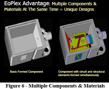
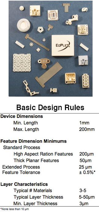
* EoPlex devices are in the size range of 5 microns to 50 millimeters and are usually referred to as miniature (not nanotechnology). There are other techniques for creating parts in this size range, but they all have limitations in handling multiple materials in the same part or in degree of geometric complexity. EoPlex fills this gap.
High-Volume Print Forming technology
“The sweet spot for the technology is parts that are about the size of paper clips,” says Arthur L. Chait, president and CEO of EoPlex, the company started by Taylor in 2001. “One thing that really differentiates this technology from rapid prototyping is the ability to use many materials.”
The process can use as many as six materials at a time, and the range of those materials is almost limitless — another huge difference from rapid prototyping.
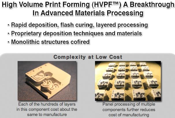
Eoplex’s proprietary print-forming technology can produce large volumes of three-dimensional structures from a wide range of metallic and non-metallic materials. The EoPlex process is called High Volume Print-Forming™ (HVPF™). It allows for thousands of small, complex structures to be built simultaneously.
A High Performance and Cost Effective Molded Array Package Substrate
This White Paper discusses a new packaging family that combines the manufacturing efficiencies of QFN with greater design flexibility and performance than BGAs and QFPs. In addition, the molded array package (MAP) substrate simplifies assembly flow and enables test in the strip prior to singulation. EoPlex’s unique print forming processes and advanced materials combine to create a MAP substrate that is more cost effective and is also very environmentally friendly in both its manufacture and use. EoPlex wishes to thank Pierangelo Magni, Mark Shaw and Maura Mazzola of STMicroelectronics for contributing their perspective
This White Paper discusses an EoPlex device that helps measure the crucial metric of tire performance and safety. This Paper covers a comprehensive field of challenges associated with TPS system development; and it explains battery limitations and owner dissatisfaction with battery replacement. Finally, this Paper explains the piezoelectric effect as the optimal candidate for energy harvesting to power TPS systems
Supporting Advertising
Trading Futures
Nano Technology
Netbook Technology News
Computer Software
Future Predictions
Thank You

Brian Wang is a Futurist Thought Leader and a popular Science blogger with 1 million readers per month. His blog Nextbigfuture.com is ranked #1 Science News Blog. It covers many disruptive technology and trends including Space, Robotics, Artificial Intelligence, Medicine, Anti-aging Biotechnology, and Nanotechnology.
Known for identifying cutting edge technologies, he is currently a Co-Founder of a startup and fundraiser for high potential early-stage companies. He is the Head of Research for Allocations for deep technology investments and an Angel Investor at Space Angels.
A frequent speaker at corporations, he has been a TEDx speaker, a Singularity University speaker and guest at numerous interviews for radio and podcasts. He is open to public speaking and advising engagements.