
J Storrs Hall has another excellent article, this one on validity of the molecular manufacturing vision and the usefulness of futurists in tough economic times. Josh states that the job of a futurist is to turn on the lights, to show what paths could actually lead to prosperity. I would say it is necessary to tap people on the shoulder and say big things are finally happening and the argument about what is or is not possible just got proven as possible. (H/t to nanowerk for many of these articles)
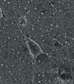
1. Carbon nanotubes connect neurons and are advancing to prosthetics for the brain. New work now considerably widens the perspectives of employing conductive nanomaterials for neuroengineering applications. It proposes carbon nanotubes not only as ideal probes for bidirectional interfaces in neuroprosthetics but also as nanotools to endogenously (re)engineer single-neuron excitability and network connectivity.
There are three fundamental obstacles to developing reliable neuroprosthetics: 1) stable interfacing of electromechanical devices with neural tissue, 2) understanding how to stimulate the neural tissue, and 3) understanding what signals to record from the neurons in order for the device to make an automatic and appropriate decision to stimulate. The new carbon nanotube-based interface technology discovered together with state of the art simulations of brain-machine interfaces is the key to developing all types of neuroprosthetics – sight, sound, smell, motion, vetoing epileptic attacks, spinal bypasses, as well as repairing and even enhancing cognitive functions.

Cultured rat hippocampal neuron grown on a layer of purified carbon nanotubes.
2. Pushing nanocrystal growth towards nanomanufacturing
Recent advance in seeded growth as the ultimate approach to producing metal nanocrystals with precisely controlled sizes, shapes, and compositions the necessary first step toward their use and assembly for large-scale applications.

3. DNA Nanotechnology goes 3D. DNA arrays assembled into a two dimensional hexagonal pattern, or a sheet, assemble further into multilayer stacks.

Unlike the formation of DNA crystals or DNA hydrogels, layer by layer assembly has an advantage as various layers can pack within three-dimensional structures, thereby providing different pore sizes for guest molecule incorporation.
There are a number of potential applications for this kind of research. One is the organization of inorganic materials on the DNA architecture, i.e. using DNA as scaffolds. Due to the multilayer packing of DNA sheets it is theoretically possible to position materials within the three dimensional framework of the DNA. The team was successful at visualizing and identifying three layers but they mention that they have also seen assemblies composed of more than three sheets.
4. Building bottom up nanowalls
New work by a team of scientists in Korea demonstrates the position- and shape-controlled growth of nanoarchitectures using the selective growth of nanowalls with conventional lithography and catalyst-free metal organic vapor-phase epitaxy (MOVPE). This presents a significant advance towards the fabrication of artificial 1D and 2D nanomaterials as functional components in many integrated electronic and photonic devices.
The most exciting scientific core of their findings is the observation of selective formation of zinc oxide (ZnO) nanowalls along pattern edges on gallium nitride/silicon (GaN/Si) substrates, which enabled us to control nucleation sites to grow nanomaterials in specific positions.

5. 
Using a process based on optical near-field effects, Lu and his team in UNL’s Laser Assisted Nano-Engineering Lab created nanoscale devices based on connecting sharp-tipped electrodes with individually self-aligned carbon nanotubes. All locations with sharp tips can accommodate carbon nanotube growth. That means we can make multiple carbon nanotubes at a time and all of them will be self-aligned.
6. Kevlar has been reinforced with carbon nanotubes.
Kevlar-CNT composites show increases in all mechanical parameters of the nanocomposite material compared to the original Kevlar fibers, e.g.: Young’s modulus, from 115 to 207 GPa; strength, from 4.7 to 5.9 GPa; strain at break, from 4.0 to 5.4%; toughness, from 63 to 99 J/g. These improvements have been achieved at only 1 – 1.75 wt% of carbon nanotube content.
Carbon nanotubes are still expensive and only a few hundred tons are made per year so being able to use them to significantly strengthen cheaper material is a good commercial thing.
7. Nanotechnology lens for ultracompact photonic devices.
While nano-patterning of optically thick metallic films was theoretically proposed as an alternative to refractive lensing, scientists at Stanford University have now reported the first experimental demonstration of far-field lensing using a plasmonic slit array. [look far away at less the wavelength of the light]
The miniaturization of lenses, for example, has been essential in the development of modern solid-state image sensors and can also have important implications for other opto-electronic applications such as displays, solid state lighting, and potentially solar cells. The focusing capability of conventional, dielectric-based microlenses however deteriorates as their physical dimensions are reduced toward a single-wavelength scale. That’s why scientists have begun exploring alternative approaches to refractive lensing.
7. Engineers use ‘nano-origami’ to build tiny electronic devices (3D MEMS and NEMS). MIT researchers folded a polymer sheet into one corner of a cube. The edge of each face is about 800 microns.
REVIEWING OTHER RECENT WORK
8. Self assembled memory is busting through what some expected was a 10-20 nanometer feature size barrier to 1-2 nanometers.
9. Room temperature single atom quantum dots
10. More durable and higher resolution nano-imprinting. It is working at 13 nanometer features and they seem confident about going to 1-2 nanometers.
11. Two Armed Nanorobotic Device Built from DNA: 100% Accurate Capture of Targeted Molecules
Chemists at New York University and China’s Nanjing University have developed a two-armed nanorobotic device that can manipulate molecules within a device built from DNA. The device is described in the latest issue of the journal Nature Nanotechnology.
13. Stanford writes 35 bits per electron

Brian Wang is a Futurist Thought Leader and a popular Science blogger with 1 million readers per month. His blog Nextbigfuture.com is ranked #1 Science News Blog. It covers many disruptive technology and trends including Space, Robotics, Artificial Intelligence, Medicine, Anti-aging Biotechnology, and Nanotechnology.
Known for identifying cutting edge technologies, he is currently a Co-Founder of a startup and fundraiser for high potential early-stage companies. He is the Head of Research for Allocations for deep technology investments and an Angel Investor at Space Angels.
A frequent speaker at corporations, he has been a TEDx speaker, a Singularity University speaker and guest at numerous interviews for radio and podcasts. He is open to public speaking and advising engagements.