

NIL already has been applied in various fields such as biological nanodevices, nanophotonic devices, organic electronics, and the patterning of magnetic materials. Researchers at Berkeley have taken this process one step further by demonstrating that direct nanoimprinting of metal nanoparticles enables low temperature metal deposition as well as high-resolution patterning. This approach has substantial potential to take advantage of nanoimprinting for the application in ultralow cost, large area printed electronics.
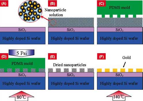
Nanoparticle nanoimprinting process. (A, B) Dispensing nanoparticle solution on SiO2/P+ Si wafer. (C, D) Pressing PDMS nanoimprinting mold on nanoparticle solution under 5 psi pressure at 80°C. (E, F) Removal of mold and induce nanoparticle melting on hot plate at 140°C. The magnified view shows the SAM protected nanoparticles suspended in organic solvent. (Reprinted with permission from American Institute of Physics)The process eliminates the need of intermediate polymer nanoimprinting steps for dry etching or vacuum deposition” says Grigoropoulos. “We effectively used a metal nanoparticle solution as a precursor to use the solution processable form of the metal component for the nanoimprinting process, thereby eliminating the need to exceed the bulk metal melting temperature. The nanoimprinted nanoparticles can be transformed into conductive and continuous metal films by low-temperature nanoparticle melting.”

Brian Wang is a Futurist Thought Leader and a popular Science blogger with 1 million readers per month. His blog Nextbigfuture.com is ranked #1 Science News Blog. It covers many disruptive technology and trends including Space, Robotics, Artificial Intelligence, Medicine, Anti-aging Biotechnology, and Nanotechnology.
Known for identifying cutting edge technologies, he is currently a Co-Founder of a startup and fundraiser for high potential early-stage companies. He is the Head of Research for Allocations for deep technology investments and an Angel Investor at Space Angels.
A frequent speaker at corporations, he has been a TEDx speaker, a Singularity University speaker and guest at numerous interviews for radio and podcasts. He is open to public speaking and advising engagements.