

The bolt on microscope resolution booster could be out to the top 1000 labs within 2 years. The target of 1 nanometer resolution for optical microscopes within 5 years looks doable.
Perhaps a Moore’s law of optical microscope resolution
2 years 70 nanometers common
3 years 20 nanometers common
4 years 8 nanometers common
5 years 4 nanometers common
6 years 2 nanometers common
7 years 1 nanometers common
Could the metamaterials allow for some advanced form of lithography ?
MIT Technology Indicates Igor Smolyaninov,University of Maryland, estimates that their method could resolve features as small as 10 nanometers.
Metamaterials are being used to extend photolithography using less extreme and more inexpensive optical sources. They call it Evanescent wave lithography. Evanescent wave lithography is different from Evanescent wave imaging. They are using projection imaging to direct images from the bottom element of the optical system through media with refractive indices lower than the numerical aperture of the imaging system,” he said. “We have been able to achieve numerical apertures up to 1.85 NA (Feb, 2006), well beyond the refractive index of any immersion fluid or photoresist currently available for 193-nm exposure. Immersion lithography is limited by Snell’s Law to numerical apertures (NA) less than the lowest refractive index material in a lithography imaging system. Currently, with fused silica optics, high-index immersion fluids, and ArF photoresists, the largest theorectical numerical aperture is about 1.65. Recently lutetium aluminum garnet (LuAG), a crystalline mineral seen by SEMATECH as the leading candidate for extending immersion lithography. LuAG has a refractive index of 2.14.
Lithography roadmap discussed in this pdf and in this article. Current research in nanolithography is reviewed by Georgia tech
Proton beams were used to demonstrate 12.5 nanometer lithography
These capabilities combined with possible large scale quantum computers show the rapidly developing tools for far more advanced work leading to molecular nanotechnology. It is becoming far more comfortable and fast for work to be done at molecular scales.
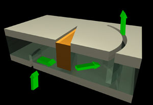
Negative refraction of green light: Light entering through a slit in the silver produces plasmons which are guided along the metal-insulator surface until they reach a gold prism embedded in the silicon nitride. Light emanates from the device at a tell-tale angle.
Lezec and co-workers have used electromagnetic waves called surface plasmons, which are generated when photons hit electrons in a metal. A layer of insulating silicon nitride is sandwiched between two sheets of silver. Light entering through a slit in the silver produces plasmons which are guided along the metal-insulator surface until they reach a gold prism embedded in the silicon nitride. As the plasmon wave passes through the 50 nanometre-wide channel between the prism and the silver sheet it is heavily perturbed, and is negatively refracted on passing back into the silcon nitride. Blue-green light emanated from the device at a tell-tale angle.
Smolyaninov’s group used a series of concentric polymer rings on a gold surface to amplify an image generated by surface plasmons.

Schematic of an optical hyperlens that can magnify and project sub-diffraction-limited objects onto a far-field plane. The objects and the hyperlens are enlarged to show details; they are actually much smaller than a conventional lens. Images courtesy the Zhang Lab, UC Berkeley. The new hyperlens, described in the Feb. 23 issue of the journal Science, is capable of projecting a magnified image of a pair of nanowires spaced 150 nanometers apart onto a plane up to a meter away.
Meanwhile Xiang Zhang and colleagues at the University of California at Berkeley captured the near-field waves and propagated them through a bulk metamaterial. Zhang used concentric cylinders to provide the optical trickery, and the incident light was just outside the visible, in the near UV. Both lenses gave resolutions of a few tens of nanometres.

Brian Wang is a Futurist Thought Leader and a popular Science blogger with 1 million readers per month. His blog Nextbigfuture.com is ranked #1 Science News Blog. It covers many disruptive technology and trends including Space, Robotics, Artificial Intelligence, Medicine, Anti-aging Biotechnology, and Nanotechnology.
Known for identifying cutting edge technologies, he is currently a Co-Founder of a startup and fundraiser for high potential early-stage companies. He is the Head of Research for Allocations for deep technology investments and an Angel Investor at Space Angels.
A frequent speaker at corporations, he has been a TEDx speaker, a Singularity University speaker and guest at numerous interviews for radio and podcasts. He is open to public speaking and advising engagements.